
Simulation Standard Technical Journal
A Journal for Process and Device Engineers
 https://silvaco.com/wp-content/uploads/simulationstandard/simstd_feb_2006_a4.jpg
1669
1344
Erick Castellon
/wp-content/uploads/2019/11/silvaco-logo.png
Erick Castellon2006-02-01 00:04:302020-09-29 23:11:41Multi-layer Organic Light Emitting Diode Simulation
https://silvaco.com/wp-content/uploads/simulationstandard/simstd_feb_2006_a4.jpg
1669
1344
Erick Castellon
/wp-content/uploads/2019/11/silvaco-logo.png
Erick Castellon2006-02-01 00:04:302020-09-29 23:11:41Multi-layer Organic Light Emitting Diode Simulation https://silvaco.com/wp-content/uploads/simulationstandard/simstd_feb_2006_a3.jpg
1669
1344
Erick Castellon
/wp-content/uploads/2019/11/silvaco-logo.png
Erick Castellon2006-02-01 00:03:042020-09-29 23:11:52Crosstalk Between Pixels of Organic Photo-Voltaic Devices
https://silvaco.com/wp-content/uploads/simulationstandard/simstd_feb_2006_a3.jpg
1669
1344
Erick Castellon
/wp-content/uploads/2019/11/silvaco-logo.png
Erick Castellon2006-02-01 00:03:042020-09-29 23:11:52Crosstalk Between Pixels of Organic Photo-Voltaic Devices https://silvaco.com/wp-content/uploads/simulationstandard/simstd_feb_2006_a2.jpg
1669
1344
Erick Castellon
/wp-content/uploads/2019/11/silvaco-logo.png
Erick Castellon2006-02-01 00:02:162020-09-29 23:13:02Athena/Optolith Simulation of Proximity Lithography
https://silvaco.com/wp-content/uploads/simulationstandard/simstd_feb_2006_a2.jpg
1669
1344
Erick Castellon
/wp-content/uploads/2019/11/silvaco-logo.png
Erick Castellon2006-02-01 00:02:162020-09-29 23:13:02Athena/Optolith Simulation of Proximity Lithography https://silvaco.com/wp-content/uploads/simulationstandard/simstd_feb_2006_a1-e1611194699264.jpg
800
600
Erick Castellon
/wp-content/uploads/2019/11/silvaco-logo.png
Erick Castellon2006-02-01 00:01:342020-09-29 23:12:56Inductance Optimization using 3D Field Solver based on Design Of Experiment Approach
https://silvaco.com/wp-content/uploads/simulationstandard/simstd_feb_2006_a1-e1611194699264.jpg
800
600
Erick Castellon
/wp-content/uploads/2019/11/silvaco-logo.png
Erick Castellon2006-02-01 00:01:342020-09-29 23:12:56Inductance Optimization using 3D Field Solver based on Design Of Experiment Approach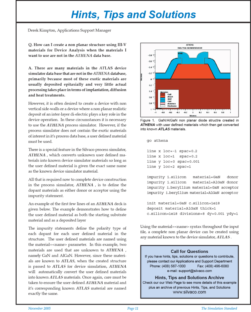 https://silvaco.com/wp-content/uploads/simulationstandard/simstd_nov_2005_hints-e1611194748751.jpg
800
644
Erick Castellon
/wp-content/uploads/2019/11/silvaco-logo.png
Erick Castellon2005-11-01 00:05:512020-09-29 23:12:46How can I create a non planar structure using III-V materials for Device Analysis
https://silvaco.com/wp-content/uploads/simulationstandard/simstd_nov_2005_hints-e1611194748751.jpg
800
644
Erick Castellon
/wp-content/uploads/2019/11/silvaco-logo.png
Erick Castellon2005-11-01 00:05:512020-09-29 23:12:46How can I create a non planar structure using III-V materials for Device Analysis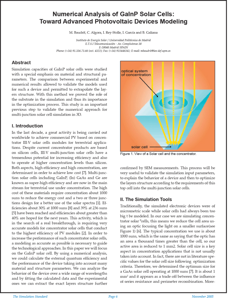 https://silvaco.com/wp-content/uploads/simulationstandard/simstd_nov_2005_a2-e1611193788843.jpg
800
644
Erick Castellon
/wp-content/uploads/2019/11/silvaco-logo.png
Erick Castellon2005-11-01 00:02:452020-09-29 23:12:40Numerical Analysis of GaInP Solar Cells: Toward Advanced Photovoltaic Devices Modeling
https://silvaco.com/wp-content/uploads/simulationstandard/simstd_nov_2005_a2-e1611193788843.jpg
800
644
Erick Castellon
/wp-content/uploads/2019/11/silvaco-logo.png
Erick Castellon2005-11-01 00:02:452020-09-29 23:12:40Numerical Analysis of GaInP Solar Cells: Toward Advanced Photovoltaic Devices Modeling