
Simulation Standard Technical Journal
A Journal for Process and Device Engineers
 https://silvaco.com/wp-content/uploads/simulationstandard/simstd_nov_2005_a1-e1611191089224.jpg
800
600
Erick Castellon
/wp-content/uploads/2019/11/silvaco-logo.png
Erick Castellon2005-11-01 00:01:312020-09-29 23:12:26Simulation and Characterization of High-Frequency Performances of Advanced MIM Capacitors
https://silvaco.com/wp-content/uploads/simulationstandard/simstd_nov_2005_a1-e1611191089224.jpg
800
600
Erick Castellon
/wp-content/uploads/2019/11/silvaco-logo.png
Erick Castellon2005-11-01 00:01:312020-09-29 23:12:26Simulation and Characterization of High-Frequency Performances of Advanced MIM Capacitors https://silvaco.com/wp-content/uploads/simulationstandard/simstd_aug_2005_hints.jpg
1669
1344
Erick Castellon
/wp-content/uploads/2019/11/silvaco-logo.png
Erick Castellon2005-08-01 00:05:122020-09-29 23:12:22How can I create a Design Of Experiments (DOE) using DeckBuild with one or more variables
https://silvaco.com/wp-content/uploads/simulationstandard/simstd_aug_2005_hints.jpg
1669
1344
Erick Castellon
/wp-content/uploads/2019/11/silvaco-logo.png
Erick Castellon2005-08-01 00:05:122020-09-29 23:12:22How can I create a Design Of Experiments (DOE) using DeckBuild with one or more variables https://silvaco.com/wp-content/uploads/simulationstandard/simstd_aug_2005_a3.jpg
1669
1344
Erick Castellon
/wp-content/uploads/2019/11/silvaco-logo.png
Erick Castellon2005-08-01 00:03:212020-09-29 23:12:17Process Flow Simulation and Manufacture of Variable RF MEMS Capacitors
https://silvaco.com/wp-content/uploads/simulationstandard/simstd_aug_2005_a3.jpg
1669
1344
Erick Castellon
/wp-content/uploads/2019/11/silvaco-logo.png
Erick Castellon2005-08-01 00:03:212020-09-29 23:12:17Process Flow Simulation and Manufacture of Variable RF MEMS Capacitors https://silvaco.com/wp-content/uploads/simulationstandard/simstd_aug_2005_a2.jpg
1669
1344
Erick Castellon
/wp-content/uploads/2019/11/silvaco-logo.png
Erick Castellon2005-08-01 00:02:072020-09-29 23:12:12Gate Charging Simulation Using Atlas/MixedMode
https://silvaco.com/wp-content/uploads/simulationstandard/simstd_aug_2005_a2.jpg
1669
1344
Erick Castellon
/wp-content/uploads/2019/11/silvaco-logo.png
Erick Castellon2005-08-01 00:02:072020-09-29 23:12:12Gate Charging Simulation Using Atlas/MixedMode https://silvaco.com/wp-content/uploads/simulationstandard/simstd_aug_2005_a1-e1611194098927.jpg
800
600
Erick Castellon
/wp-content/uploads/2019/11/silvaco-logo.png
Erick Castellon2005-08-01 00:01:162020-09-29 23:12:07Using Athena Monte Carlo Module for Ion Implantation Simulation in Silicon Carbides
https://silvaco.com/wp-content/uploads/simulationstandard/simstd_aug_2005_a1-e1611194098927.jpg
800
600
Erick Castellon
/wp-content/uploads/2019/11/silvaco-logo.png
Erick Castellon2005-08-01 00:01:162020-09-29 23:12:07Using Athena Monte Carlo Module for Ion Implantation Simulation in Silicon Carbides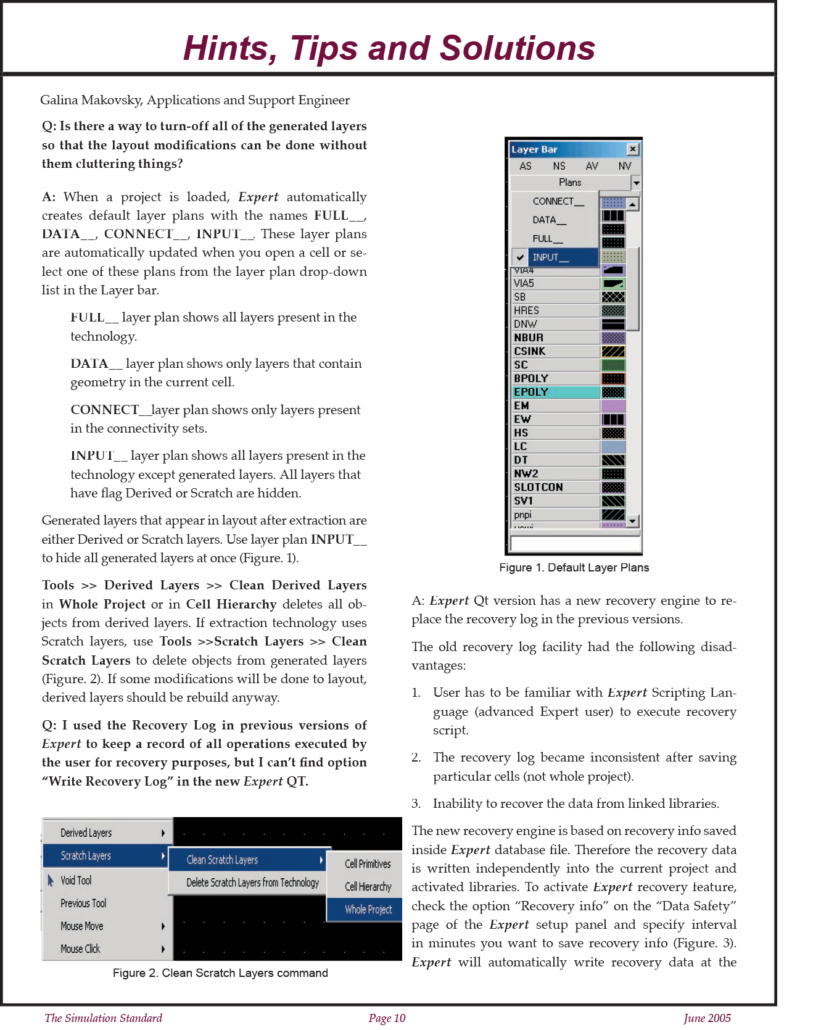 https://silvaco.com/wp-content/uploads/simulationstandard/simstd_jun_2005_hints.jpg
1669
1344
Erick Castellon
/wp-content/uploads/2019/11/silvaco-logo.png
Erick Castellon2005-06-01 00:05:572020-10-01 21:56:06Is there a way to turn-off all of the generated layers
https://silvaco.com/wp-content/uploads/simulationstandard/simstd_jun_2005_hints.jpg
1669
1344
Erick Castellon
/wp-content/uploads/2019/11/silvaco-logo.png
Erick Castellon2005-06-01 00:05:572020-10-01 21:56:06Is there a way to turn-off all of the generated layers