Simulation Standard Technical Journal
A Journal for Process and Device Engineers
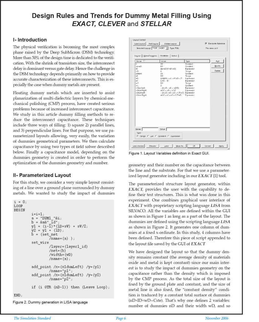
Design Rules and Trends for Dummy Metal Filling Using Exact, Clever and Stellar
Introduction
The physical verification is becoming the most complex phase raised by the Deep SubMicron (DSM) technology. More than 50% of the design time is dedicated to the verification. With the shrink of transistors size, the interconnect delay is dominant versus gate delay. Hence the challenge in the DSM technology depends primarily on how to provide accurate characterization of these interconnects. This is especially the case when dummy metals are present.
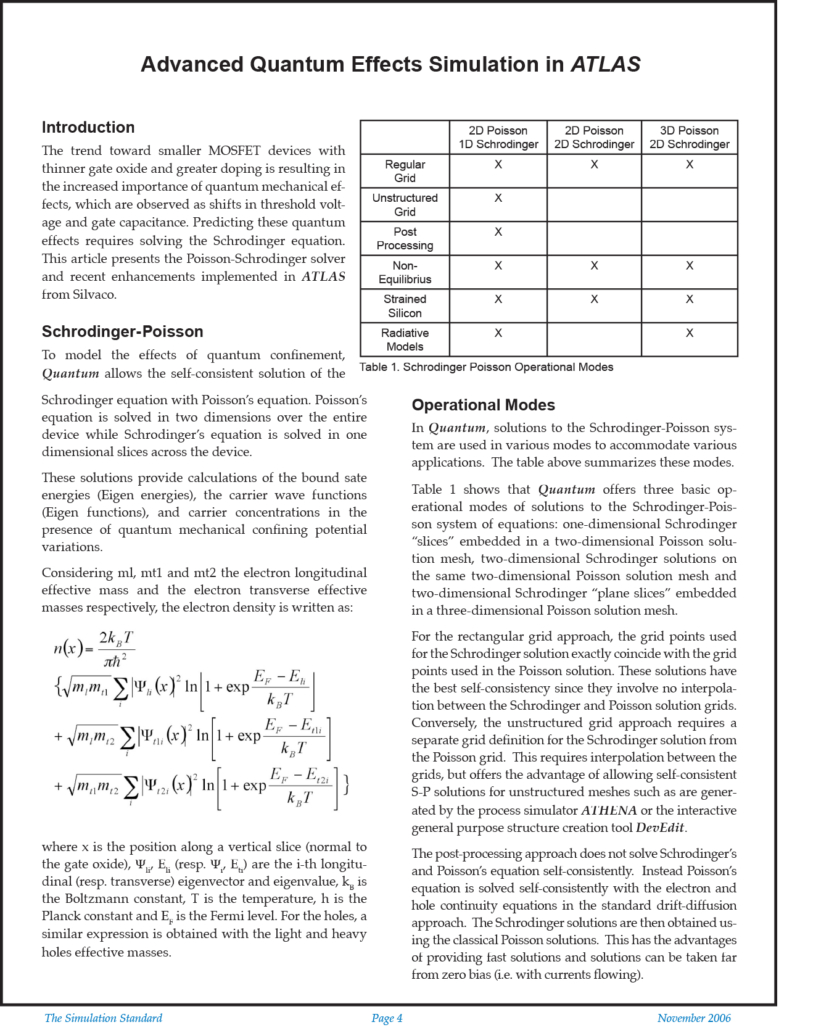
Advanced Quantum Effects Simulation in Atlas
Introduction
The trend toward smaller MOSFET devices with thinner gate oxide and greater doping is resulting in the increased importance of quantum mechanical effects, which are observed as shifts in threshold voltage and gate capacitance. Predicting these quantum effects requires solving the Schrodinger equation. This article presents the Poisson-Schrodinger solver and recent enhancements implemented in ATLAS from Silvaco.
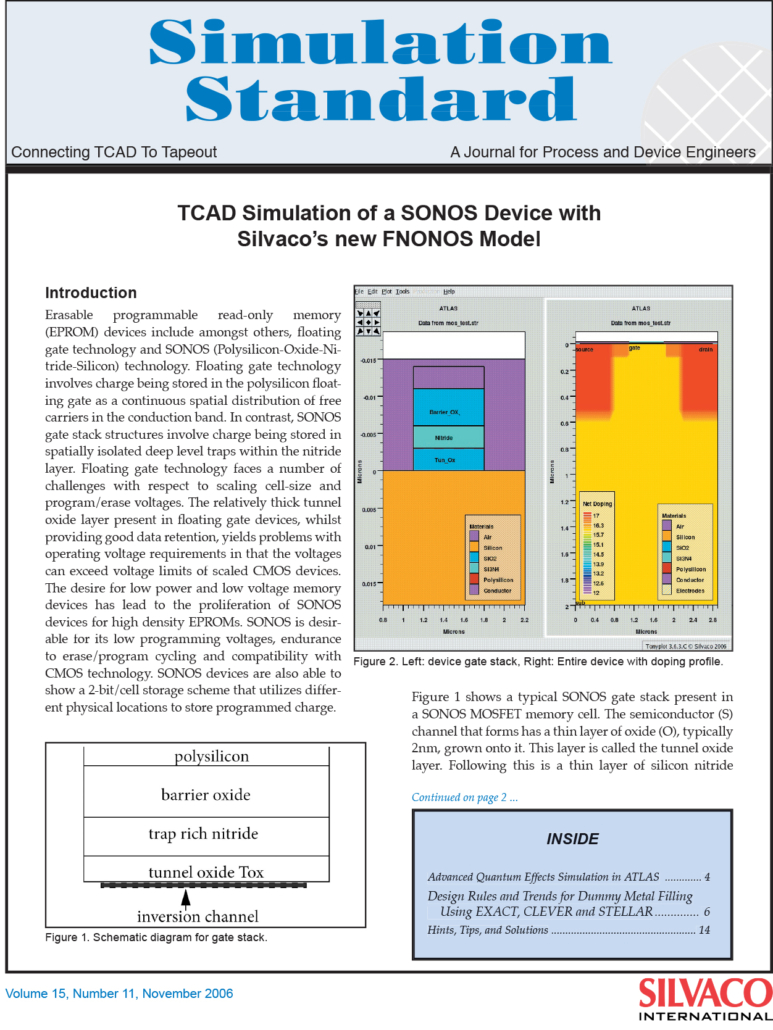
TCAD Simulation of a SONOS Device with Silvaco’s new FNONOS Model
Introduction
Erasable programmable read-only memory (EPROM) devices include amongst others, floating gate technology and SONOS (Polysilicon-Oxide-Nitride-Silicon) technology. Floating gate technology involves charge being stored in the polysilicon floating gate as a continuous spatial distribution of free carriers in the conduction band. In contrast, SONOS gate stack structures involve charge being stored in spatially isolated deep level traps within the nitride layer.
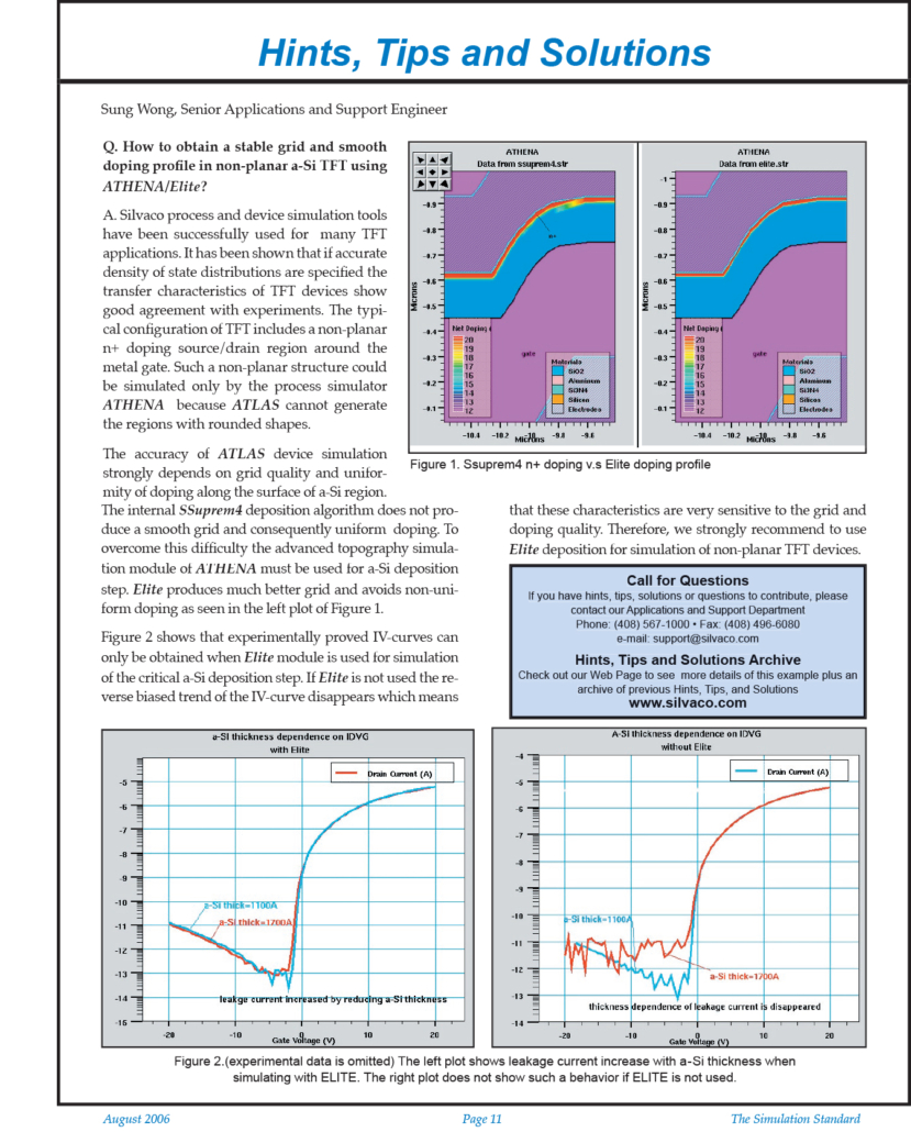
How to obtain a stable grid and smooth doping profile in non-planar a-Si TFT using Athena/Elite?
How to obtain a stable grid and smooth doping profile in non-planar a-Si TFT using Athena/Elite?
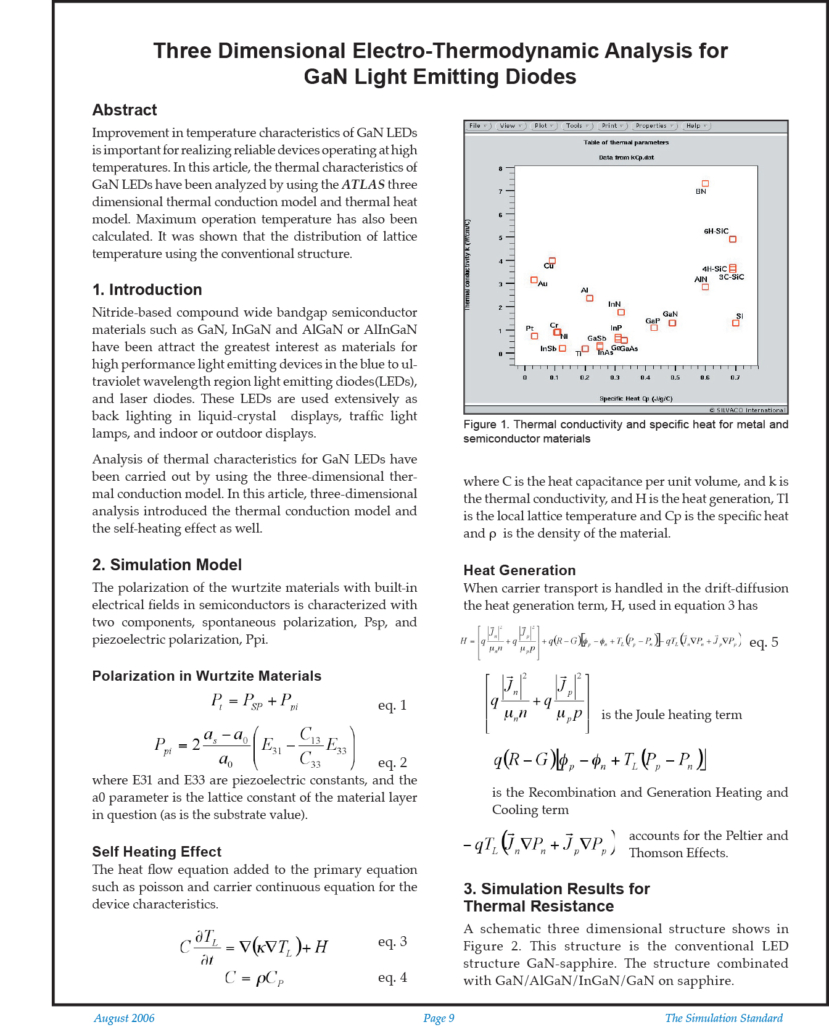
Three Dimensional Electro-Thermodynamic Analysis for GaN Light Emitting Diodes
Abstract
Improvement in temperature characteristics of GaN LEDs is important for realizing reliable devices operating at high temperatures. In this article, the thermal characteristics of GaN LEDs have been analyzed by using the ATLAS three dimensional thermal conduction model and thermal heat model. Maximum operation temperature has also been calculated. It was shown that the distribution of lattice temperature using the conventional structure.
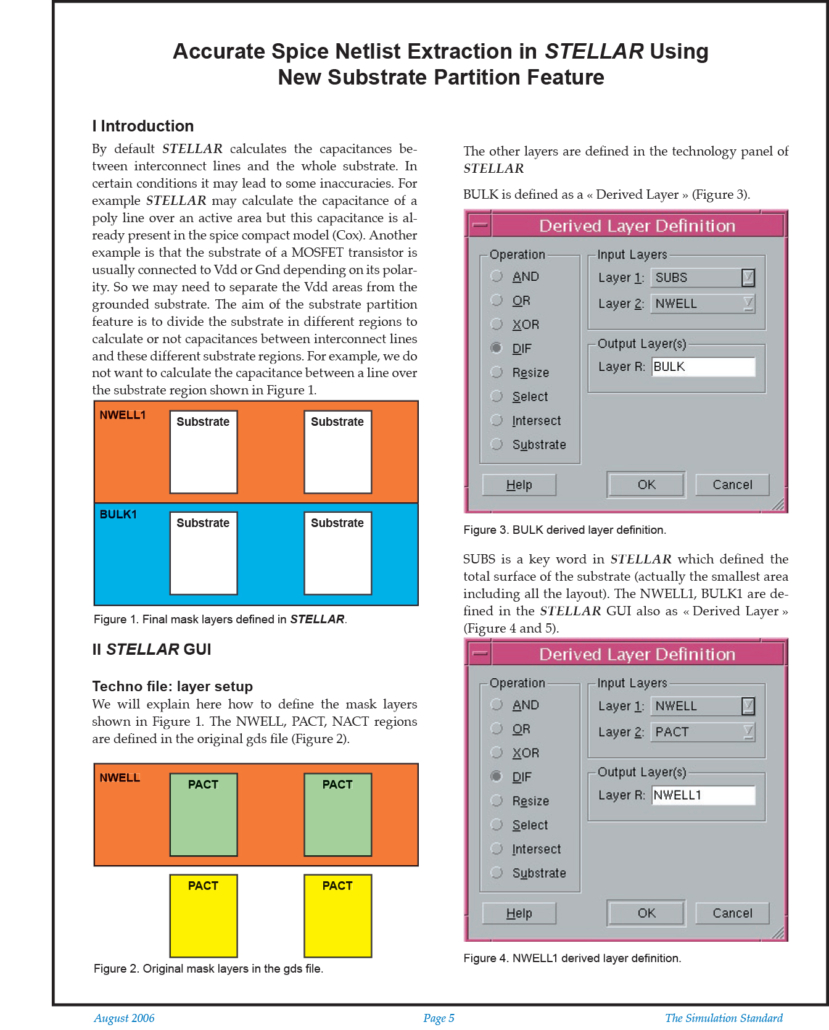
Accurate Spice Netlist Extraction in Stellar Using New Substrate Partition Feature
Introduction
By default STELLAR calculates the capacitances between interconnect lines and the whole substrate. In certain conditions it may lead to some inaccuracies. For example STELLAR may calculate the capacitance of a poly line over an active area but this capacitance is already present in the spice compact model (Cox). Another example is that the substrate of a MOSFET transistor is usually connected to Vdd or Gnd depending on its polarity.

