
Simulation Standard Technical Journal
A Journal for Process and Device Engineers
 https://silvaco.com/wp-content/uploads/2020/03/simstd_Q3_2010_a1.jpg
1012
782
Ingrid Schwarz
/wp-content/uploads/2019/11/silvaco-logo.png
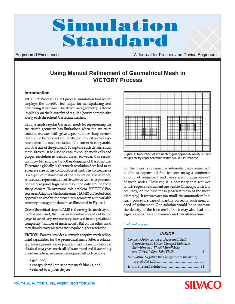
Ingrid Schwarz2010-07-01 16:02:392020-12-22 09:55:37Using Manual Refinement of Geometrical Mesh in VICTORY Process
https://silvaco.com/wp-content/uploads/2020/03/simstd_Q3_2010_a1.jpg
1012
782
Ingrid Schwarz
/wp-content/uploads/2019/11/silvaco-logo.png
Ingrid Schwarz2010-07-01 16:02:392020-12-22 09:55:37Using Manual Refinement of Geometrical Mesh in VICTORY Process https://silvaco.com/wp-content/uploads/2020/03/simstd_Q2_2010_a3.jpg
1012
782
Ingrid Schwarz
/wp-content/uploads/2019/11/silvaco-logo.png
Ingrid Schwarz2010-04-01 15:52:182020-12-22 11:26:17Simulating the Hysteresis effects of Si/SiO2 Interface Traps
https://silvaco.com/wp-content/uploads/2020/03/simstd_Q2_2010_a3.jpg
1012
782
Ingrid Schwarz
/wp-content/uploads/2019/11/silvaco-logo.png
Ingrid Schwarz2010-04-01 15:52:182020-12-22 11:26:17Simulating the Hysteresis effects of Si/SiO2 Interface Traps https://silvaco.com/wp-content/uploads/2020/03/simstd_Q2_2010_a2.jpg
1012
782
Ingrid Schwarz
/wp-content/uploads/2019/11/silvaco-logo.png
Ingrid Schwarz2010-04-01 15:45:572020-12-21 12:50:40Designing a High-Voltage IGBT Structure with TCAD
https://silvaco.com/wp-content/uploads/2020/03/simstd_Q2_2010_a2.jpg
1012
782
Ingrid Schwarz
/wp-content/uploads/2019/11/silvaco-logo.png
Ingrid Schwarz2010-04-01 15:45:572020-12-21 12:50:40Designing a High-Voltage IGBT Structure with TCAD https://silvaco.com/wp-content/uploads/2020/03/simstd_Q2_2010_a1.jpg
1012
782
Ingrid Schwarz
/wp-content/uploads/2019/11/silvaco-logo.png
Ingrid Schwarz2010-04-01 15:01:092020-12-22 16:50:30Investigation of the SiGe Waveguide Photodiodes Using FDTD Method for High Speed Optical Communication
https://silvaco.com/wp-content/uploads/2020/03/simstd_Q2_2010_a1.jpg
1012
782
Ingrid Schwarz
/wp-content/uploads/2019/11/silvaco-logo.png
Ingrid Schwarz2010-04-01 15:01:092020-12-22 16:50:30Investigation of the SiGe Waveguide Photodiodes Using FDTD Method for High Speed Optical Communication https://silvaco.com/wp-content/uploads/2020/03/simstd_Q1_2010_a4.jpg
1012
782
Ingrid Schwarz
/wp-content/uploads/2019/11/silvaco-logo.png
Ingrid Schwarz2010-01-01 14:58:562020-12-20 16:25:18A Box Method Discretisation for the Drift-Diffusion Equations in a Magnetic Field
https://silvaco.com/wp-content/uploads/2020/03/simstd_Q1_2010_a4.jpg
1012
782
Ingrid Schwarz
/wp-content/uploads/2019/11/silvaco-logo.png
Ingrid Schwarz2010-01-01 14:58:562020-12-20 16:25:18A Box Method Discretisation for the Drift-Diffusion Equations in a Magnetic Field https://silvaco.com/wp-content/uploads/2020/03/simstd_Q1_2010_a3.jpg
1012
782
Ingrid Schwarz
/wp-content/uploads/2019/11/silvaco-logo.png
Ingrid Schwarz2010-01-01 14:50:102021-01-11 12:46:49Simulation of Resonant Tunneling Diodes Using ATLAS
https://silvaco.com/wp-content/uploads/2020/03/simstd_Q1_2010_a3.jpg
1012
782
Ingrid Schwarz
/wp-content/uploads/2019/11/silvaco-logo.png
Ingrid Schwarz2010-01-01 14:50:102021-01-11 12:46:49Simulation of Resonant Tunneling Diodes Using ATLAS