Simulation Standard Technical Journal
A Journal for Process and Device Engineers

Using VICTORY PROCESS for Rapid Geometry Prototyping
The fully three-dimensional process simulator VICTORY PROCESS allows user to perform a wide range of manipulations of the structure’s geometry in order to obtain the device of the desired shape. Most of the supported operations correspond to real technological processes (etching or deposition, CMP, epitaxy and others) so in many cases an engineer can establish a direct link between the technological processes step and an input deck statement of VICTORY PROCESS.
3D SOI NMOSFET Simulation Using VICTORY DEVICE
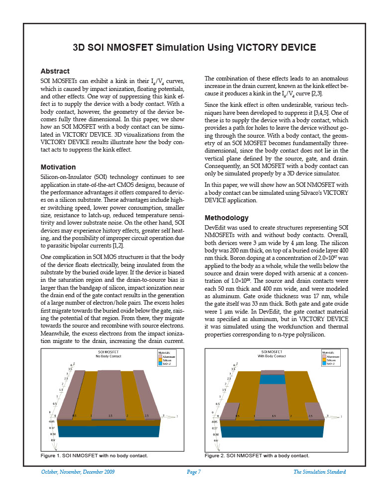
SOI MOSFETs can exhibit a kink in their Id/Vd curves, which is caused by impact ionization, floating potentials, and other effects. One way of suppressing this kink effect is to supply the device with a body contact. With a body contact, however, the geometry of the device becomes fully three dimensional. In this paper, we show how an SOI MOSFET with a body contact can be simulated in VICTORY DEVICE. 3D visualizations from the VICTORY DEVICE results illustrate how the body contact acts to suppress the kink effect.
Crosstalk Simulation in InSb Detector Arrays
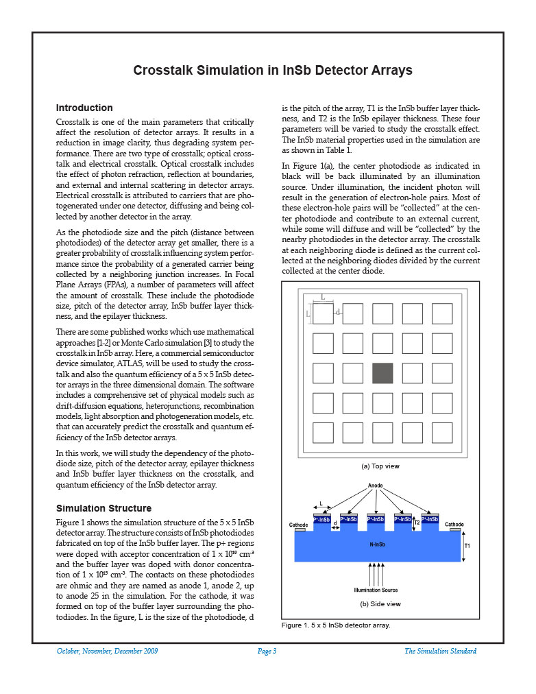
Crosstalk is one of the main parameters that critically affect the resolution of detector arrays. It results in a reduction in image clarity, thus degrading system performance. There are two type of crosstalk; optical crosstalk and electrical crosstalk. Optical crosstalk includes the effect of photon refraction, reflection at boundaries, and external and internal scattering in detector arrays. Electrical crosstalk is attributed to carriers that are photogenerated under one detector, diffusing and being collected by another detector in the array.
Simulating the Effects of Stress/Strain on a 50 nm Silicon FinFET
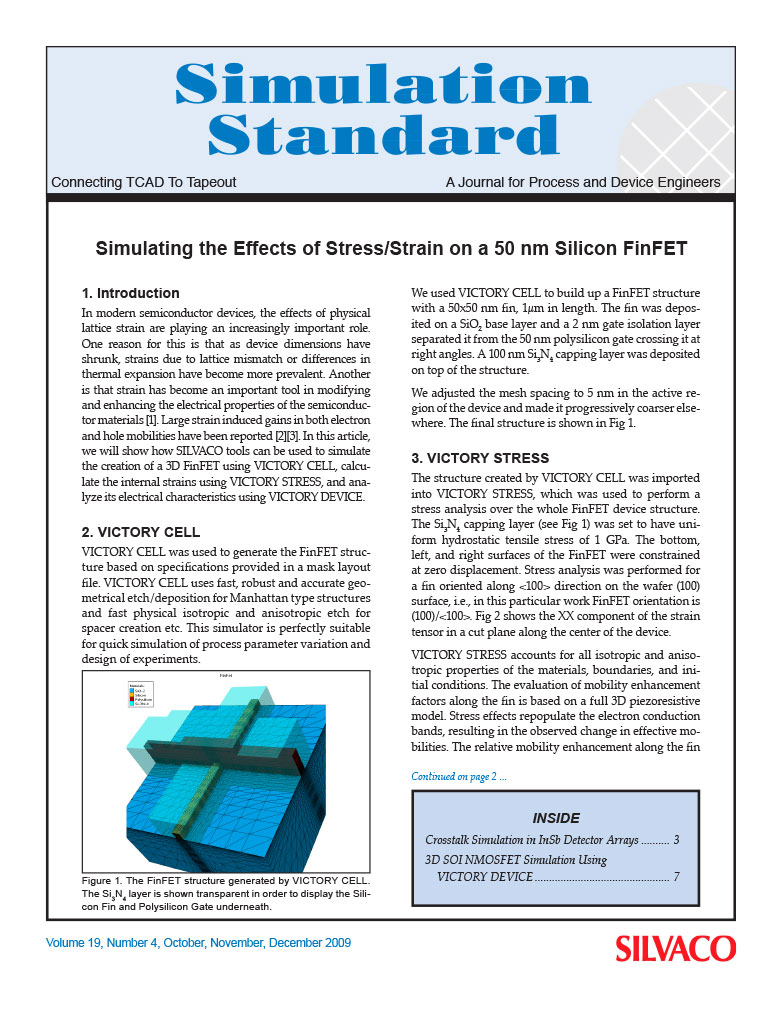
In modern semiconductor devices, the effects of physical lattice strain are playing an increasingly important role. One reason for this is that as device dimensions have shrunk, strains due to lattice mismatch or differences in thermal expansion have become more prevalent. Another is that strain has become an important tool in modifying and enhancing the electrical properties of the semiconductor materials [1]. Large strain induced gains in both electron and hole mobilities have been reported [2][3]. In this article, we will show how SILVACO tools can be used to simulate the creation of a 3D FinFET using VICTORY CELL, calculate the internal strains using VICTORY STRESS, and analyze its electrical characteristics using VICTORY DEVICE.
Textured Thin-film Solar Cell Simulation
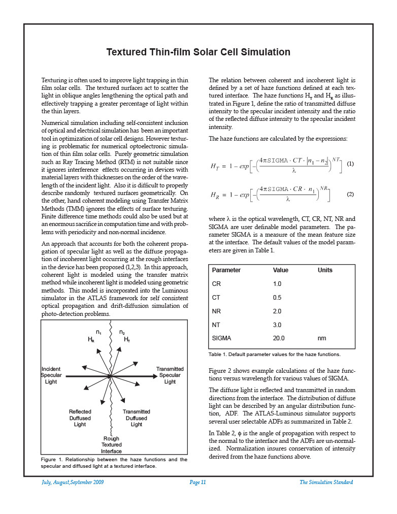
Texturing is often used to improve light trapping in thin film solar cells. The textured surfaces act to scatter the light in oblique angles lengthening the optical path and effectively trapping a greater percentage of light within the thin layers.
Evaluating of the Breakdown Voltage of the Super-Junctions Using ATLAS
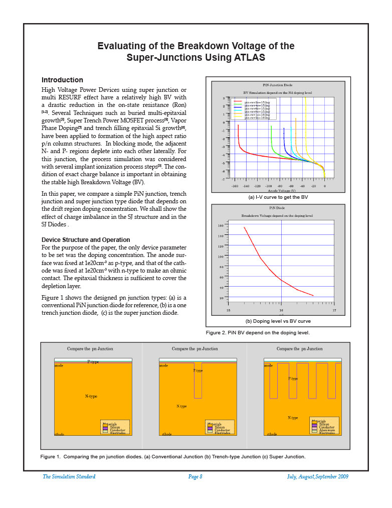
High Voltage Power Devices using super junction or multi RESURF effect have a relatively high BV with a drastic reduction in the on-state resistance (Ron)[1-2]. Several Techniques such as buried multi-epitaxial growth[3], Super Trench Power MOSFET process[4], Vapor Phase Doping[5] and trench filling epitaxial Si growth[6], have been applied to formation of the high aspect ratio p/n column structures. In blocking mode, the adjacent N- and P- regions deplete into each other laterally. For this junction, the process simulation was considered with several implant ionization process steps[3]. The condition of exact charge balance is important in obtaining the stable high Breakdown Voltage (BV).

