Simulation Standard
Silvaco面向半导体工艺和器件仿真工程师推出的技术刊物
Inter-Tool Communication Within CAD CELEBRITY
One of the main features of modern complex Computer-Aided Design Systems is the ability to support the communication between concurrently executing applications within the design process. This feature allows applications, intended for different steps in a design flow, to exchange design data in an integrated manner and therefore to solve design tasks more accurately, easily and quickly.
Hints, Tips, and Solutions February 2000
Q. How can I ensure that the vertical Y.MESH spacing in my process simulation is adequate for my particular implant condition? A. A good technique to check that the mesh is not causing a problem is to perform an integration of the as-implanted species, directly after the implant within ATHENA.
Reverse Engineering An AlGaAs/InGaAs PHEMT With FastBlaze
FastBlaze is an ultra-fast physical MESFET and HEMT simulator which incorporates advanced physical models. By designing the simulator and its framework specifically for these devices, Silvaco has optimized device simulation algorithms and data structures for high speed without sacrificing the accuracy of the physical models.
ATLAS Field Dependent Mobility: Model Parameters for (0001) 6H-SiC and (0001) 4H-SiC
For high temperature, high power applications Silicon Carbide (SiC) continues to be a useful material for device fabrication because of its wide band gap, high breakdown field, and high thermal conductivity [1]. Some common power devices utilizing SiC include the following: Schottky and p-n junction diodes, thyristors, and UMOSFETs. Recent research has further contributed to the characterization of the electrical transport properties of 6H-SiC and 4H-SiC [2].
Investigating Two Dimensional Implantation Effects Using The BCA Model
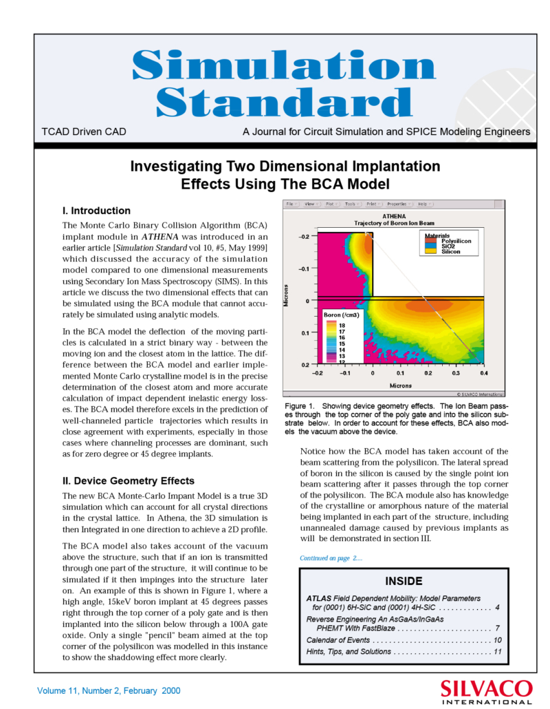
The Monte Carlo Binary Collision Algorithm (BCA) implant module in ATHENA was introduced in an earlier article [Simulation Standard Vol 10, #5, May 1999] which discussed the accuracy of the simulation model compared to one dimensional measurements using Secondary Ion Mass Spectroscopy (SIMS). In this article we discuss the two dimensional effects that can be simulated using the BCA module that cannot accurately be simulated using analytic models.
Hints & Tips January 1999
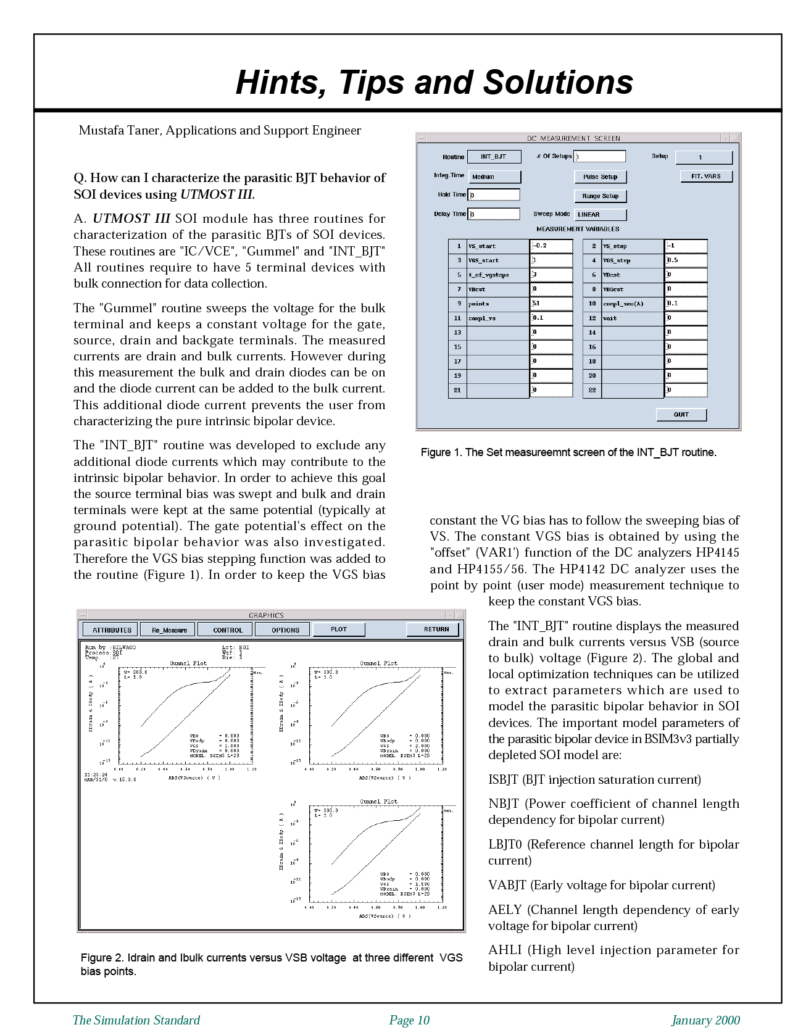
A. UTMOST III SOI module has three routines for characterization of the parasitic BJTs of SOI devices. These routines are "IC/VCE", "Gummel" and "INT_BJT" All routines require to have 5 terminal devices with bulk connection for data collection.

