Simulation Standard
Silvaco面向半导体工艺和器件仿真工程师推出的技术刊物
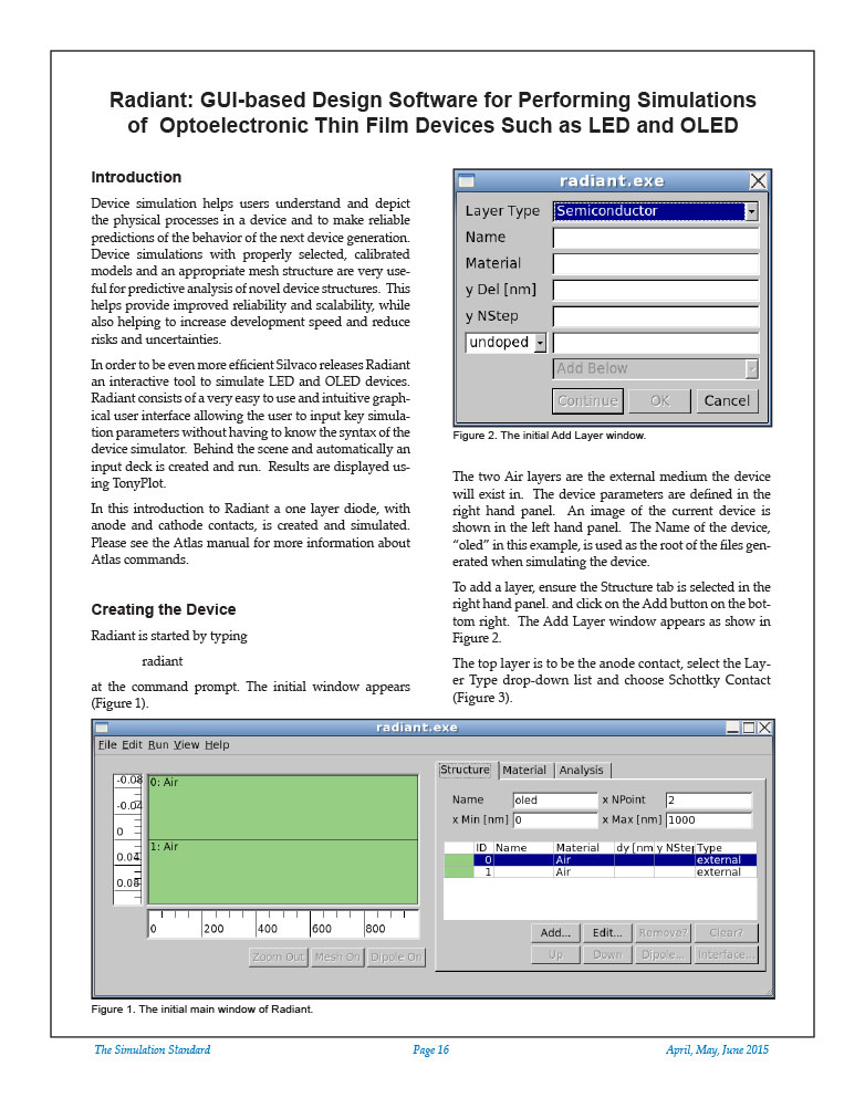
Radiant: GUI-based Design Software for Performing Simulations of Optoelectronic Thin Film Devices Such as LED and OLED
Device simulation helps users understand and depict the physical processes in a device and to make reliable predictions of the behavior of the next device generation. Device simulations with properly selected, calibrated models and an appropriate mesh structure are very useful for predictive analysis of novel device structures. This helps provide improved reliability and scalability, while also helping to increase development speed and reduce risks and uncertainties.
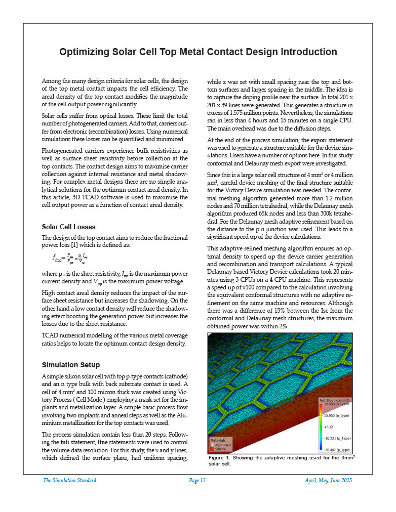
Optimizing Solar Cell Top Metal Contact Design Introduction
Among the many design criteria for solar cells, the design of the top metal contact impacts the cell efficiency. The areal density of the top contact modifies the magnitude of the cell output power significantly.
Vertical LOCOS Power Devices in Victory Process: From 3D Process and Electrical Optimisation to High Speed, Full Chip Process Emulation
There is a constant demand to lower the on-state resistance of devices, improving their energy efficiency as well as increasing their current handling capabilities whilst maintaining the desired breakdown voltage. However, a trade-off relationship exists between the on-state resistance and breakdown voltage. This is referred to as the silicon limit [1]. Attempts have been made to break the silicon limit. One such method proposed by several authors is the Vertical LOCOS MOS (VLOCOS) [2,3].
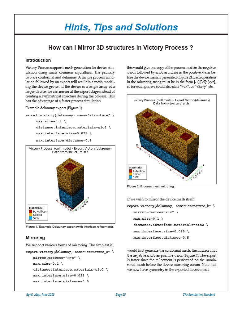
Hints, Tips and Solutions – Mirror 3D structures in Victory Process
Victory Process supports mesh generation for device simulation using many common algorithms. The primary two are conformal and delaunay. A simple process simulation followed by an export will result in a mesh modeling the device grown. If the device is a single array of a larger device, we can mirror at the export stage instead of creating a symmetrical structure during the process. This has the advantage of a faster process simulation.
Plasmonic Light Trapping Transforming Thin-Film Photovoltaics
The photovoltaics (PV) market represents the fastest growing renewable energy technology, with a 35% annual growth rate, which is projected to be worth $150B by 2018.[1] The global cumulative installed PV capacity has exceeded 140 GW in 2013 and is generating 160 TWh/year of electricity, representing 0.85% of worldwide electricity demand. At the present growth rate, it is projected that over 20% of all electricity could be supplied by PV by 2050[1].
Hints, Tips, and Solutions – Defining VWF Curve Target For Curve Calibration
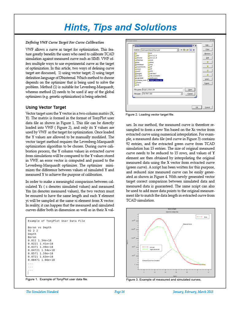
VWF allows a curve as target for optimization. This feature greatly benefits the users who need to calibrate TCAD simulation against measured curve such as SIMS. VWF offers multiple ways to use experimental curve as the target of optimization. In this article, two ways of defining curve target are discussed, 1) using vector target; 2) using target definition language of Dbinternal. Which method to choose depends on the optimizer that is being used to solve the problem. Method (1) is suitable for Levenberg-Marquardt, whereas method (2) needs to be used if any of the global optimizers (e.g. genetic optimization) is being selected.

