
Simulation Standard
Technical Journal
A Journal for Process and Device Engineers
 https://silvaco.com/wp-content/uploads/simulationstandard/simstd_feb_2003_a1.jpg
1669
1302
Graham Bell
/wp-content/uploads/2019/11/silvaco-logo.png
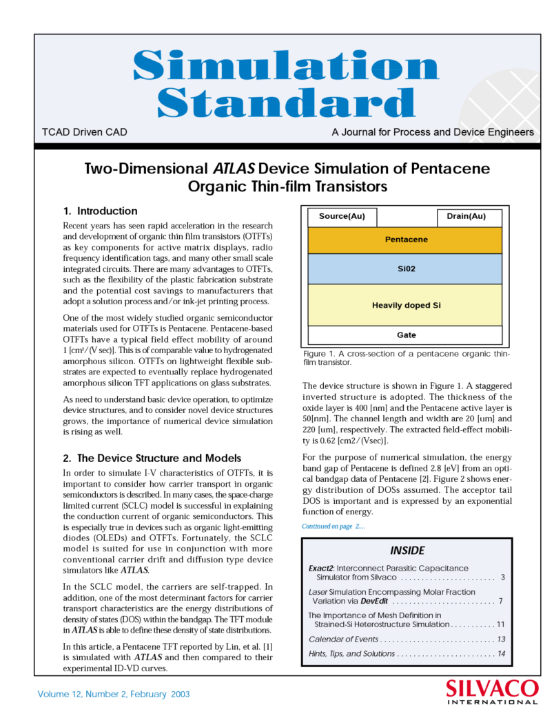
Graham Bell2003-02-01 23:06:392020-12-22 10:03:48Two-Dimensional ATLAS Device Simulation of Pentacene Organic Thin-film Transistors
https://silvaco.com/wp-content/uploads/simulationstandard/simstd_feb_2003_a1.jpg
1669
1302
Graham Bell
/wp-content/uploads/2019/11/silvaco-logo.png
Graham Bell2003-02-01 23:06:392020-12-22 10:03:48Two-Dimensional ATLAS Device Simulation of Pentacene Organic Thin-film Transistors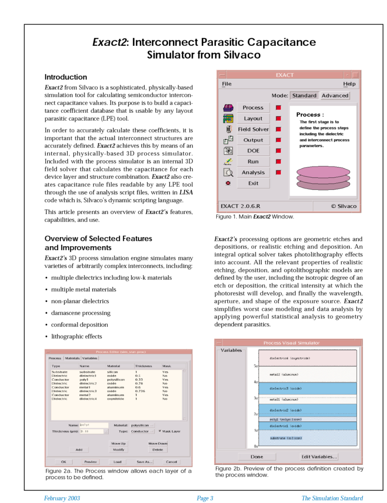 https://silvaco.com/wp-content/uploads/simulationstandard/simstd_feb_2003_a2.jpg
1669
1287
Graham Bell
/wp-content/uploads/2019/11/silvaco-logo.png
Graham Bell2003-02-01 22:11:472020-12-22 15:39:47Exact2: Interconnect Parasitic Capacitance Simulator
https://silvaco.com/wp-content/uploads/simulationstandard/simstd_feb_2003_a2.jpg
1669
1287
Graham Bell
/wp-content/uploads/2019/11/silvaco-logo.png
Graham Bell2003-02-01 22:11:472020-12-22 15:39:47Exact2: Interconnect Parasitic Capacitance Simulator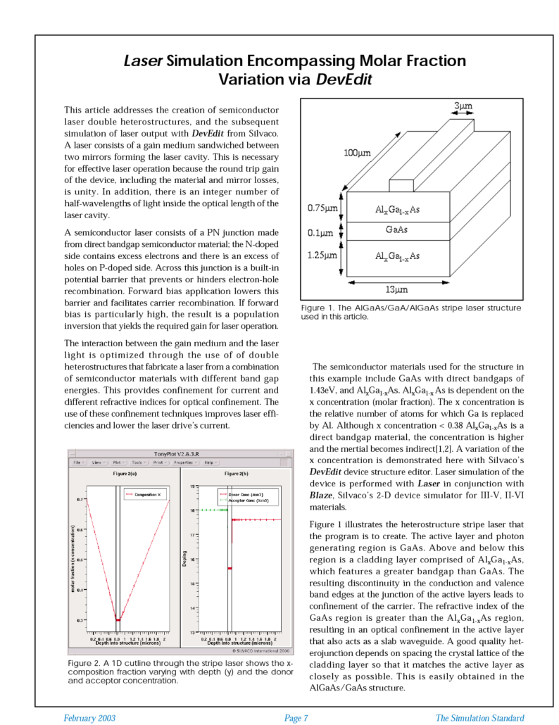 https://silvaco.com/wp-content/uploads/simulationstandard/simstd_feb_2003_a3.jpg
1669
1287
Graham Bell
/wp-content/uploads/2019/11/silvaco-logo.png
Graham Bell2003-02-01 21:16:212021-01-22 14:03:25Laser Simulation Encompassing Molar Fraction Variation via DevEdit
https://silvaco.com/wp-content/uploads/simulationstandard/simstd_feb_2003_a3.jpg
1669
1287
Graham Bell
/wp-content/uploads/2019/11/silvaco-logo.png
Graham Bell2003-02-01 21:16:212021-01-22 14:03:25Laser Simulation Encompassing Molar Fraction Variation via DevEdit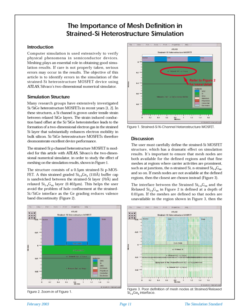 https://silvaco.com/wp-content/uploads/simulationstandard/simstd_feb_2003_a4-e1611193315648.jpg
800
617
Graham Bell
/wp-content/uploads/2019/11/silvaco-logo.png
Graham Bell2003-02-01 20:20:372020-12-22 10:16:45The Importance of Mesh Definition in Strained-Si Heterostructure Simulation
https://silvaco.com/wp-content/uploads/simulationstandard/simstd_feb_2003_a4-e1611193315648.jpg
800
617
Graham Bell
/wp-content/uploads/2019/11/silvaco-logo.png
Graham Bell2003-02-01 20:20:372020-12-22 10:16:45The Importance of Mesh Definition in Strained-Si Heterostructure Simulation https://silvaco.com/wp-content/uploads/simulationstandard/simstd_feb_2003_hints.jpg
1669
1286
Graham Bell
/wp-content/uploads/2019/11/silvaco-logo.png
Graham Bell2003-02-01 19:23:562020-12-22 12:32:43Optical Lithography Models in ATHENA
https://silvaco.com/wp-content/uploads/simulationstandard/simstd_feb_2003_hints.jpg
1669
1286
Graham Bell
/wp-content/uploads/2019/11/silvaco-logo.png
Graham Bell2003-02-01 19:23:562020-12-22 12:32:43Optical Lithography Models in ATHENA