
Simulation Standard Technical Journal
A Journal for Process and Device Engineers
 https://silvaco.com/wp-content/uploads/2020/03/simstd_Q2_2014_hints1.jpg
1012
782
Ingrid Schwarz
/wp-content/uploads/2019/11/silvaco-logo.png
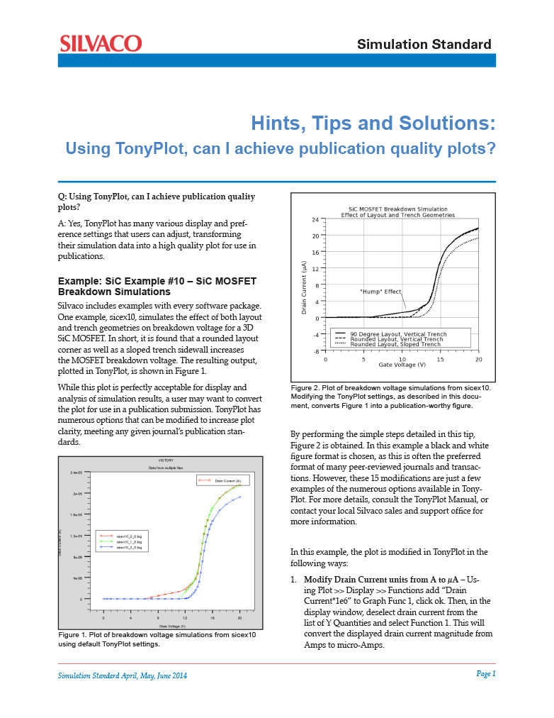
Ingrid Schwarz2014-04-01 19:34:052021-01-22 14:13:46Hints, Tips, and Solutions – Achieve Publication Quality Plots Using TonyPlot
https://silvaco.com/wp-content/uploads/2020/03/simstd_Q2_2014_hints1.jpg
1012
782
Ingrid Schwarz
/wp-content/uploads/2019/11/silvaco-logo.png
Ingrid Schwarz2014-04-01 19:34:052021-01-22 14:13:46Hints, Tips, and Solutions – Achieve Publication Quality Plots Using TonyPlot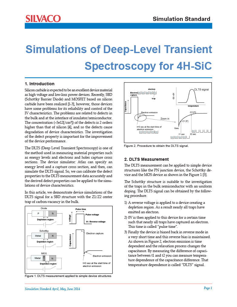 https://silvaco.com/wp-content/uploads/2020/03/simstd_Q2_2014_a2.jpg
1012
782
Ingrid Schwarz
/wp-content/uploads/2019/11/silvaco-logo.png
Ingrid Schwarz2014-04-01 19:30:312020-12-22 10:58:29Simulations of Deep-Level Transient Spectroscopy for 4H-SiC
https://silvaco.com/wp-content/uploads/2020/03/simstd_Q2_2014_a2.jpg
1012
782
Ingrid Schwarz
/wp-content/uploads/2019/11/silvaco-logo.png
Ingrid Schwarz2014-04-01 19:30:312020-12-22 10:58:29Simulations of Deep-Level Transient Spectroscopy for 4H-SiC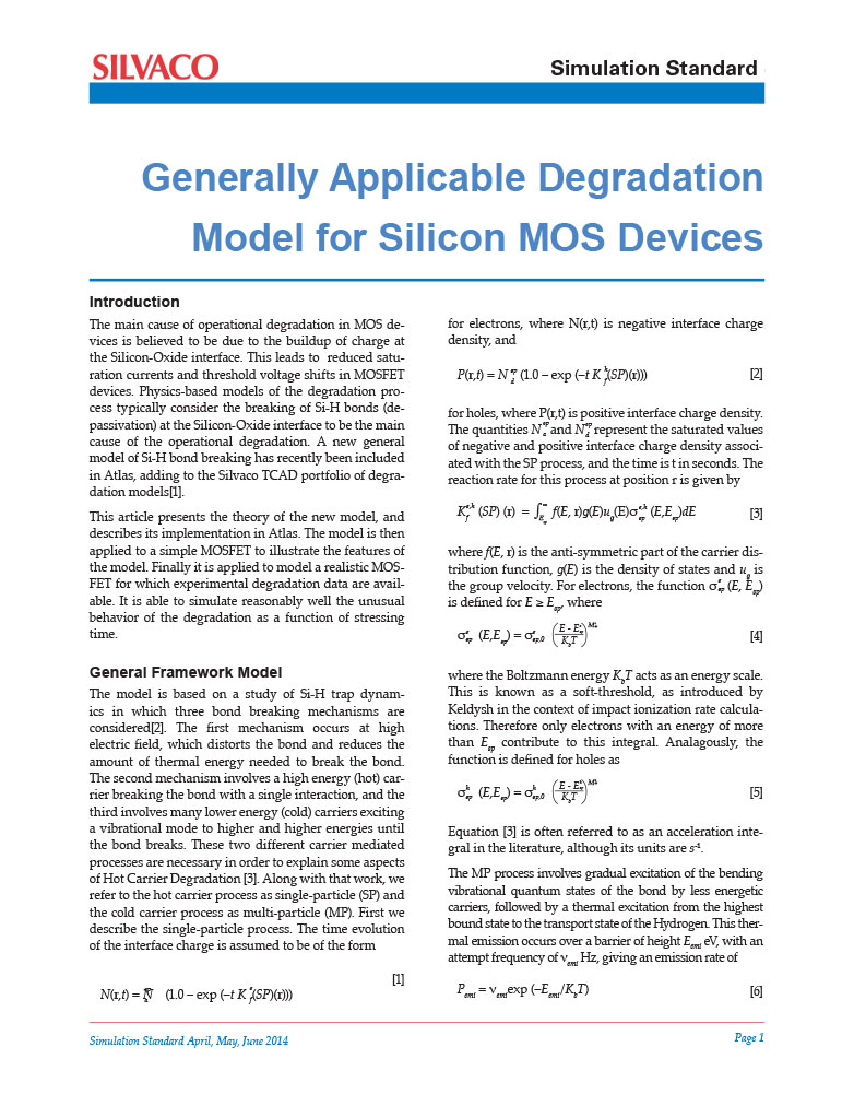 https://silvaco.com/wp-content/uploads/2020/03/simstd_Q2_2014_a1.jpg
1012
782
Ingrid Schwarz
/wp-content/uploads/2019/11/silvaco-logo.png
Ingrid Schwarz2014-04-01 19:23:362020-12-22 16:46:43Generally Applicable Degradation Model for Silicon MOS Devices
https://silvaco.com/wp-content/uploads/2020/03/simstd_Q2_2014_a1.jpg
1012
782
Ingrid Schwarz
/wp-content/uploads/2019/11/silvaco-logo.png
Ingrid Schwarz2014-04-01 19:23:362020-12-22 16:46:43Generally Applicable Degradation Model for Silicon MOS Devices https://silvaco.com/wp-content/uploads/2020/03/simstd_Q1_2014_hints2.jpg
1012
782
Ingrid Schwarz
/wp-content/uploads/2019/11/silvaco-logo.png
Ingrid Schwarz2014-01-01 19:04:132020-12-22 16:46:56Hints, Tips, and Solutions – Simulation on a Cluster of Computers Using the Distributed Computing Feature
https://silvaco.com/wp-content/uploads/2020/03/simstd_Q1_2014_hints2.jpg
1012
782
Ingrid Schwarz
/wp-content/uploads/2019/11/silvaco-logo.png
Ingrid Schwarz2014-01-01 19:04:132020-12-22 16:46:56Hints, Tips, and Solutions – Simulation on a Cluster of Computers Using the Distributed Computing Feature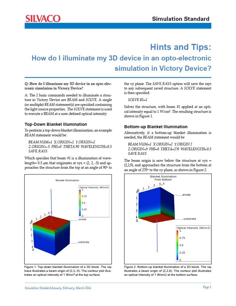 https://silvaco.com/wp-content/uploads/2020/03/simstd_Q1_2014_hints1.jpg
1012
782
Ingrid Schwarz
/wp-content/uploads/2019/11/silvaco-logo.png
Ingrid Schwarz2014-01-01 18:35:432020-12-22 10:57:45Hints, Tips and Solutions – Illuminate a 3D device in a Victory Device Opto-electronic Simulation
https://silvaco.com/wp-content/uploads/2020/03/simstd_Q1_2014_hints1.jpg
1012
782
Ingrid Schwarz
/wp-content/uploads/2019/11/silvaco-logo.png
Ingrid Schwarz2014-01-01 18:35:432020-12-22 10:57:45Hints, Tips and Solutions – Illuminate a 3D device in a Victory Device Opto-electronic Simulation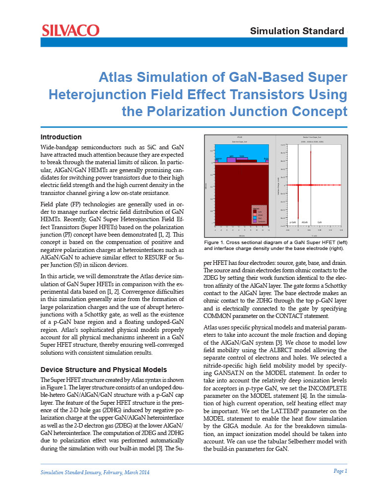 https://silvaco.com/wp-content/uploads/2020/03/simstd_Q1_2014_a2.jpg
1012
782
Ingrid Schwarz
/wp-content/uploads/2019/11/silvaco-logo.png
Ingrid Schwarz2014-01-01 14:52:202021-01-11 12:14:07Atlas Simulation of GaN-Based Super Heterojunction Field Effect Transistors Using the Polarization Junction Concept
https://silvaco.com/wp-content/uploads/2020/03/simstd_Q1_2014_a2.jpg
1012
782
Ingrid Schwarz
/wp-content/uploads/2019/11/silvaco-logo.png
Ingrid Schwarz2014-01-01 14:52:202021-01-11 12:14:07Atlas Simulation of GaN-Based Super Heterojunction Field Effect Transistors Using the Polarization Junction Concept