
Simulation Standard
Silvaco面向半导体工艺和器件仿真工程师推出的技术刊物
 https://silvaco.com/wp-content/uploads/2020/03/simstd_Q3_2016_a2-1.jpg
1012
782
Ingrid Schwarz
/wp-content/uploads/2019/11/silvaco-logo.png
Ingrid Schwarz2016-07-01 18:33:502021-10-13 09:55:25Simulation of Device Degradation Due to Bias Temperature Stress
https://silvaco.com/wp-content/uploads/2020/03/simstd_Q3_2016_a2-1.jpg
1012
782
Ingrid Schwarz
/wp-content/uploads/2019/11/silvaco-logo.png
Ingrid Schwarz2016-07-01 18:33:502021-10-13 09:55:25Simulation of Device Degradation Due to Bias Temperature Stress https://silvaco.com/wp-content/uploads/2020/03/simstd_Q3_2016_a1-1.jpg
1012
782
Ingrid Schwarz
/wp-content/uploads/2019/11/silvaco-logo.png
Ingrid Schwarz2016-07-01 18:04:512021-10-13 09:55:26Using Victory Process to Create Realistic Structures for Capacitance Extraction in Clever
https://silvaco.com/wp-content/uploads/2020/03/simstd_Q3_2016_a1-1.jpg
1012
782
Ingrid Schwarz
/wp-content/uploads/2019/11/silvaco-logo.png
Ingrid Schwarz2016-07-01 18:04:512021-10-13 09:55:26Using Victory Process to Create Realistic Structures for Capacitance Extraction in Clever https://silvaco.com/wp-content/uploads/2020/03/simstd_Q3_2016_hints1-1.jpg
1012
782
Ingrid Schwarz
/wp-content/uploads/2019/11/silvaco-logo.png
Ingrid Schwarz2016-07-01 10:11:552023-04-26 10:19:25Hints, Tips and Solutions – How to best visualize vectors and field lines in TonyPlot
https://silvaco.com/wp-content/uploads/2020/03/simstd_Q3_2016_hints1-1.jpg
1012
782
Ingrid Schwarz
/wp-content/uploads/2019/11/silvaco-logo.png
Ingrid Schwarz2016-07-01 10:11:552023-04-26 10:19:25Hints, Tips and Solutions – How to best visualize vectors and field lines in TonyPlot https://silvaco.com/wp-content/uploads/2020/03/simstd_Q3_2016_hints-1.jpg
1012
782
Ingrid Schwarz
/wp-content/uploads/2019/11/silvaco-logo.png
Ingrid Schwarz2016-07-01 10:08:212023-04-26 10:17:01Hints, Tips and Solutions – Scattering mechanisms contributing to reduced channel mobility in 4H-SiC MOSFETs
https://silvaco.com/wp-content/uploads/2020/03/simstd_Q3_2016_hints-1.jpg
1012
782
Ingrid Schwarz
/wp-content/uploads/2019/11/silvaco-logo.png
Ingrid Schwarz2016-07-01 10:08:212023-04-26 10:17:01Hints, Tips and Solutions – Scattering mechanisms contributing to reduced channel mobility in 4H-SiC MOSFETs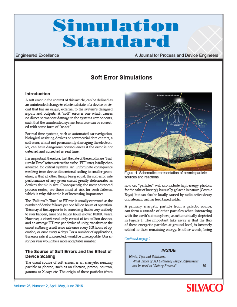 https://silvaco.com/wp-content/uploads/2020/03/simstd_Q2_2016_a1-1.jpg
1012
782
Ingrid Schwarz
/wp-content/uploads/2019/11/silvaco-logo.png
Ingrid Schwarz2016-04-01 17:13:512021-10-13 09:57:24Soft Error
https://silvaco.com/wp-content/uploads/2020/03/simstd_Q2_2016_a1-1.jpg
1012
782
Ingrid Schwarz
/wp-content/uploads/2019/11/silvaco-logo.png
Ingrid Schwarz2016-04-01 17:13:512021-10-13 09:57:24Soft Error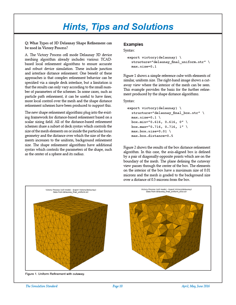 https://silvaco.com/wp-content/uploads/2020/03/simstd_Q2_2016_hints-1.jpg
1012
782
Ingrid Schwarz
/wp-content/uploads/2019/11/silvaco-logo.png
Ingrid Schwarz2016-04-01 10:47:422021-10-13 09:57:24Hints, Tips and Solutions – Types of 3D Delaunay Shape Refinement
https://silvaco.com/wp-content/uploads/2020/03/simstd_Q2_2016_hints-1.jpg
1012
782
Ingrid Schwarz
/wp-content/uploads/2019/11/silvaco-logo.png
Ingrid Schwarz2016-04-01 10:47:422021-10-13 09:57:24Hints, Tips and Solutions – Types of 3D Delaunay Shape Refinement