For Next Generation Nanowires, Simulation from Atoms to SPICE
With this extra requirement for additional physics for all stages of the design flow in mind, we must have a single design interactive environment to flow seamlessly from 3D process and device physics based TCAD, to final SPICE circuit simulation including SPICE model parameter extraction from the TCAD simulations. The modularity of the flow also allows entire sections of the flow to be left out if not required. For example, if SPICE model cards are sufficiently accurate, the designer can omit the TCAD sections of the flow and concentrate on design optimization on circuit performance.
Here, a 3D atomistic to SPICE circuit simulation flow is demonstrated. It allows investigation of impact different variables of interest can have on the final circuit performance. Aspects such as process parameters, SPICE model fitting sequence, and changes in circuit configuration, can all be investigated through a single design environment. The tool flow sequence and user choices for each step are outlined in this article. The general DTCO flow is illustrated in Fig. 1.
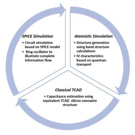
Figure 1. Complete process flow from Atomistic simulation to SPICE modeling.
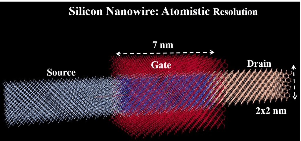
Figure2. Atomistic representation of silicon nanowire FET with 7nm channel, 2nm width and 2nm thickness.
To read the rest of this Simulation Standard article go to Next Generation CMOS Nanowire: From Atoms to Circuit Simulation.
