TCAD Modeling and Data of NOR Nanocrystal Memories
S. Jacob (1, 2), L. Perniola(1), P. Scheiblin(1), B. De Salvo(1), G. Lecarval(1), E. Jalaguier(1), G. Festes(2), R. Coppard(2), F. Boulanger(1), S. Deleonibus(1)
(1) CEA-LETI, 17 rue des Martyrs, 38054 Grenoble Cedex 9, France, stephanie.jacob@cea.fr(2) ATMEL Rousset, Zone industrielle, 13790 Rousset, France
Introduction
It is widely believed that the scaling of standard Flash devices will face in a near future several limitations, due to the high voltage requirement of the program/erase and the stringent charge storage requirement of the dielectrics [1]. Among the possible solutions to push further the scaling limits of standard technologies, Si nanocrystal (Si-NC) memories are one of the most promising. It has been shown that thanks to the discrete nature of Si-NC, thinner tunnel oxide can be used (allowing lower operating voltages), without compromising the reliability [2, 3]. Indeed, a first understanding of the Si-NC memory behaviour can be achieved through simplified/semianalytical models [4, 5, 6]. Nevertheless, these approaches are not enough accurate to allow the optimization of the technological parameters, especially for NOR cells, written by channel hot electron (CHE) injection. To this aim, more complex numerical models, which take into account twodimensional (2D) or even three-dimensional (3D) effects, should be used.
In this work, we present TCAD simulations of NOR NC memories performed with commercial tools, which allow for a good understanding of the impact of the localized charge on both electrostatics and dynamics of the cell. Correlations with experimental results will be also presented.
Devices and Simulation Tools
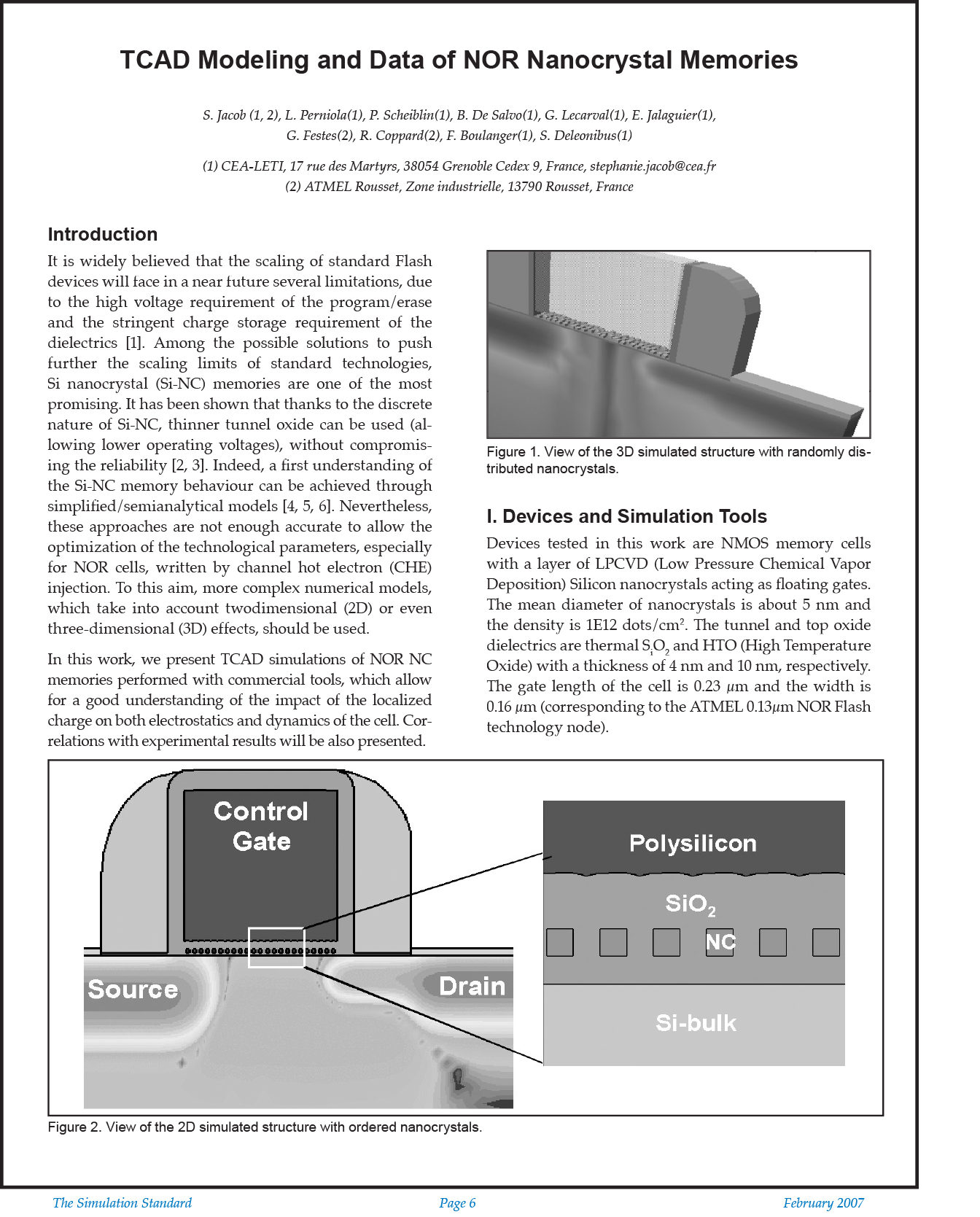
Devices tested in this work are NMOS memory cells with a layer of LPCVD (Low Pressure Chemical Vapor Deposition) Silicon nanocrystals acting as floating gates. The mean diameter of nanocrystals is about 5 nm and the density is 1E12 dots/cm2. The tunnel and top oxide dielectrics are thermal SiO2 and HTO (High Temperature Oxide) with a thickness of 4 nm and 10 nm, respectively. The gate length of the cell is 0.23 µm and the width is 0.16 µm (corresponding to the ATMEL 0.13µm NOR Flash technology node).
Two- and three-dimensional simulations have been performed with commercial TCAD tools [7]. Structures fed to the device simulator, including doping profiles, were obtained from 2D process simulations (2D profiles were then extruded in the third dimension for 3D simulations). In the simulated devices, nanocrystals are approximated as metallic cubes with 5 nm edge and a density of 1E12 dots/cm2.
Electrostatic Simulations
A. Comparison between a 3D “random-distributed” NC memory cell and a 2D “ordered” NC memory cell
A three-dimensional structure, where the embedded nanocrystals are randomly distributed (both along the device length and width), was firstly simulated (see Fig.1). Indeed, this structure resembles the actual device, but 3D simulations imply high computational burdens. To bypass this limit, a 2D NC device (see Fig.2), where the embedded nanocrystals are ordered (i.e. equally spaced along the cell length and extending like rod structures along the device width) was also simulated. Due to the ordered nanocrystal configuration, in 2D uniformly charged devices, the trapped electrons give rise to a wave-like modulation of the surface potential along the device length, while creating a uniform potential barrier over the device width. An agreement between electrical results of the 2D and 3D structures should be quantitatively demonstrated.


