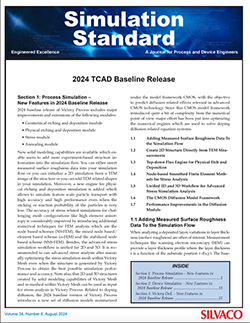
2024 TCAD基准版本软件发布
- 第一部分:Victory Process——2024基准版本中的新功能
- 第二部分:Victory Device——2024基准版本中的新功能
- 第三部分:Victory DoE——2024基准版本中的新功能

How Can I Re-Use Individual Monte-Carlo 3D Implant Profiles?
It is often the case that a design of experiments (DOE) is required to optimize the performance of a particular device. Sometimes this simply means tweaking the implant dose for threshold voltage or other minor adjustments, but in other cases it can mean tweaking such things as high energy deep well implants.
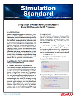
Comparison of Models for Fluorine Effect on Dopant Diffusion in CMOS Processes
Recently a new diffusion model was introduced to Victory Process: the CMOS model. This model aims at taking on the challenges brought by the specificities of CMOS device processing such as steep temperature ramps, short annealings or shallow implantations.
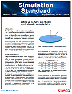
Setting up the Wafer Orientation: Applications to Ion Implantation
Properly setting the wafer orientation in Victory Process (VP) is critical for various processes such as ion implantation, etching, and deposition. For ion implantation in particular, the determination of the wafer orientation becomes crucial, given its profound impact on profile variations in channeling and non-channeling directions.
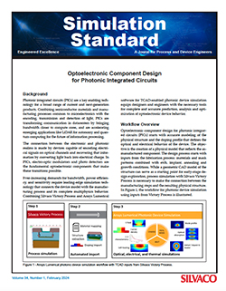
Optoelectronic Component Design for Photonic Integrated Circuits
Photonic integrated circuits (PICs) are a key enabling technology for a broad range of current and next-generation products. Combining semiconductor materials and manufacturing processes common to microelectronics with the encoding, transmission and detection of light, PICs are transforming communication in datacenters by bringing bandwidth closer to compute cores, and are accelerating emerging applications like LiDAR for autonomy and quantum computing for the future of information processing.
Advanced TCAD Modeling of HfO2-based ReRAM: Coupling Redox Reactions and Thermal Effects
This paper presents a TCAD modeling approach for HfO2-based ReRAM (Resistive Random Access Memory). For describing the switching and retention behaviors of a ReRAM cell, the proposed model includes the essential redox reactions coupled to an electron transport model and to heat generation. The effects of various parameters such as sweep time, and device geometry on the switching behavior are investigated. Simulation results demonstrate that thermal management is crucial both for the reliable operation of ReRAM cells and retention. The proposed TCAD model provides insight into the design and optimization of HfO2-based ReRAM devices.
Numerical Algorithm to Perform Viscoelastic Analysis
Numerical Algorithm to Perform Viscoelastic Analysis
Viscous materials exhibit both viscous and elastic characteristics when undergoing deformation. The response of such materials to force is characterized by two distinct phases. The materials first deform instantaneously akin to elastic materials. Following on, the material continues to deform at a relatively slower time scale. Typically, materials undergoing thermal treatment exhibit viscoelastic properties.
2023 TCAD Baseline Release
New Features in the 2023 Baseline Release:
- Section 1: Process Simulation – New Features in 2023 Baseline Release
- Section 2: Device Simulation – New Features in 2023 Baseline Release
- Section 3: Victory Mesh – New Features in 2023 Baseline Release
- Section 4: New Examples in 2023 Baseline Release
Simulation Framework for Device-packaging Co-design for Power Electronics
The past several years has seen a fast deployment of wide-bandgap power devices in fast chargers, electric vehicles, data centers and renewable energy processing. The performance of power devices is fast progressing towards their intrinsic material limit. As these devices can handle higher voltage and larger current density, packaging and thermal management will become the key limiting factor for exploiting their benefits in power electronic converters and systems.
Understanding of Geometrical Boundary Conditions in Victory Process
It is common to run the process simulation for the part of a larger structure just to reduce the computation time. To account for the influence of parts of the structure outside the simulation domain, Victory Process makes assumptions about overall structure geometry.
