
GaN-based Power Devices Design and Development with Silvaco TCAD Solution
 A large amount of research effort has been invested over the last two decades in wide bandgap GaN-based lateral power devices, which are currently approaching commercial maturity for power electronic switching up to the 650 V class. However, they do not approach their theoretical material limit in terms of RDS_ON × A vs. VBr. Among the reasons for this limitation are tradeoffs between the blocking strength and the increase of dispersion and the vertical blocking strength of GaN on Si substrates.
Among the different approaches to overcome these challenges, two device technologies may be highlighted: vertical GaN based devices and ultra-wideband gap lateral HFET with AlN buffer.
Vertical GaN-based transistors are desired due to their reduced wafer “footprint” in comparison to lateral HFETs. That results in a reduction of RDS_ON × A by one order of magnitude, down to 1.0 mΩ∙cm2. In addition, the possibility of strain-free homoepitaxy allows the growth of thick drift layers with low residual background doping for blocking capability larger than 1 kV.
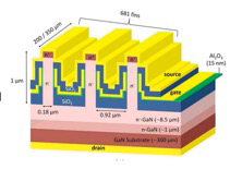
Lateral GaN based transistors (HFETs) with unintentional doped AlN as buffer material and with high conduction band offset at the AlN-buffer / GaN channel interface should effectively confine the GaN transistor channel. This will result in blocking strength enhancement and low dispersion effects.
Physical-based simulation tools are essential for the development and insight to these new generation of wide band gap electronic devices in FBH laboratories. In this webinar, we will give examples for the use of Silvaco simulation tools used to design, predict, and analysis the electrical characterization of vertical and lateral GaN based power devices.
The conductance properties of GaN based fin MISFETs are explored and compared to experimental characteristics. The conductance properties are predicted with the variation of geometrical dimensions and the epitaxial layers properties. Edge termination topologies in vertical GaN devices are engineered using avalanche models and compared to experimental and theoretical values.
Finally, insight to trapping and de-trapping effects AlN / GaN lateral HFET provides explanations to dynamic ON state resistance peculiarity using avalanche models specific to the device epitaxial structure.
What You Will Learn
- Vertical GaN fin-MISFET channel conductance
- Fin geometry and epitaxy design
- Vertical GaN devices drift region and edge termination design
- Lateral AIN / GaN / AlGAN HFETs for high voltage switching
- Insights into trapping and de-trapping effects
Presenter
Dr. Eldad Bahat-Treidel, Senior Scientist, Ferdinand-Braun-Institut (FBH)
Eldad Bahat-Treidel received his B.Sc. degree in chemical process engineering and M.Sc. degree in electro-optic engineering from Ben Gurion University, Be’er Sheva, Israel in 1996 and 2004 respectively. He received his Ph.D. ( Dr. Ing. ) in electrical engineering from the Technische Universität Berlin Germany in 2012. In 1996 he joined Intel electronics LTD as a photolithography critical layers process engineer, and then joined in 2004 Tower semiconductor LTD as a senior research and development photolithography engineer. In 2006 he joined the Ferdinand-Braun-Institut gGmbH, Leibniz-Institut für Höchstfrequenztechnik (FBH) in Berlin for the development of GaN switching transistors for high voltage power electronics applications. Since 2014 he has been working on the research and development of innovative electronic devices such vertical GaN based transistors.
WHO SHOULD ATTEND:
Semiconductor Device and Process engineers, product managers, and engineering management.
When: February 29, 2024
Where: Online
Times:
10:00 Santa Clara
11:00 Paris
10:00 Beijing
Language: English