Victory Process
Victory Process 2D and 3D Layout-Driven Simulator
TCAD Process simulation is crucial to develop new technologies, as well as maintain existing semiconductor processes. Virtualizing the manufacturing process allows organizations to maintain a “digital twin” of their semiconductor process. Changes in process can be well understood; maximizing device performance, increase manufacturing yield, while minimizing number of engineering cycles and cycle time.
Benefits
- Allow optimization of existing processes and provides predictive scaling behavior
- Increase understanding of novel technology challenges
- Reduce mask and prototyping foundry cost by replacing experiments by simulation
- Reduce time-to-market by creation of virtual process based PDK prior to silicon for fabless companies
Typical Applications
- Advanced CMOS: FinFET, FDSOI, Bulk CMOS
- Display technology: TFT, LED, OLED
- Power & RF technologies: Silicon BiCMOS and BCD, SiC, GaN
- Optical and photonics: CIS, Solar Cell, Laser, Waveguides, Modulators
Core Functionality
- Automatic switching between 1D, 2D and 3D modes
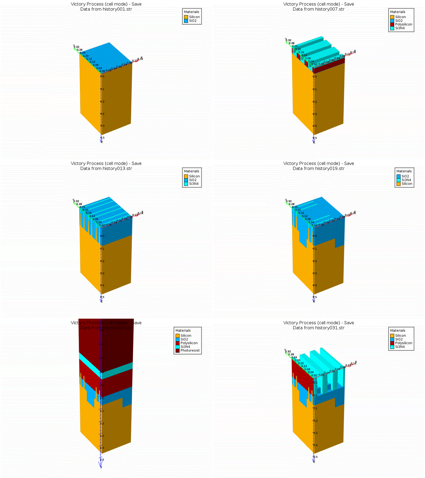
- Masked-based process simulation, with direct import of GDSII layouts
- Integration within Silvaco TCAD flow
- Run simulations and analyze results with TCAD Interactive tools
- Set up Design of Experiments and Optimization routines with Virtual Wafer Fab
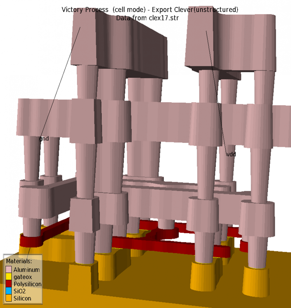
- Export results to TCAD Device Simulation, or for 3D RC extraction
- High performance due to efficient multi-threading
- Open Model Interface to add new semiconductor process physics
- Open Material Database to add new materials and parameters
Ion Implantation
Analytical implantation mode
- Experimentally verified Pearson and double-Pearson analytical models, including user-defined moments
- Import doping profiles
- Analytical profiles (Gaussian, ERFC)
Monte-Carlo (MC) implantation mode
- Binary Collision Approximation Monte Carlo calculations for crystalline and amorphous materials
- Universal tilt and rotation capability for Monte Carlo calculations
- Empirical models for implantation induced crystal damage; Plus-one model for point defect, <311> cluster model
Dopant Diffusion & Activation
- Impurity diffusion in general multi-material structures in 1D, 2D, and 3D
- Comprehensive set of default models:
- Direct / Fick model, Fermi model, Fully Coupled model, Five-stream model, Single-pair model, Single-pair model for interstitial supersaturation, Two-Dimensional model, Grain-based polysilicon model
- Empirical and transient activation models
- Point defect trapping and clustering models
- Coupled with oxidation&oxidation enhanced diffusion
- Open modeling interface for user-defined diffusion and activation models
- Open and flexible material database for modeling parameters
Oxidation
- Calibrated Silicon and Silicon Carbide oxidation
- No limitation on materials that can be oxidized. Expansion via Open Model Interface and Open Material Database
- Three modes of operation:
- Analytical, Empirical (Massoud Model), & Full physical mode
- In the full physical mode
- the oxygen transport and material flow are solved numerically
- Stress calculation including impact on oxidation characteristics
- Influence of the ambient composition
- Crystal orientation effects
- Influence of doping on the oxidation rate
Deposition & Epitaxy
- Fast geometrical deposition models for structure prototyping
- Physical conformal and non-conformal deposition models with selectivity
- Physical directional deposition models. Shading and visibility effects are taken into account at feature level
- Secondary effects are taken into account, including reflection of deposited material
- Multi-particle physical deposition models are supported
- Ion beam deposition model with comprehensive beam control, material-specific tabulated sticking functions
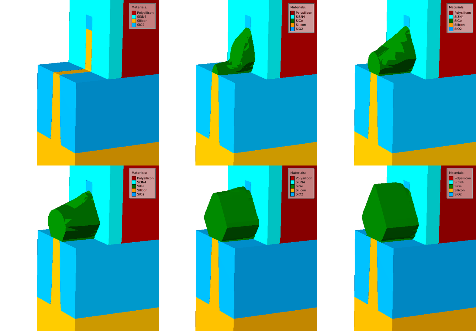
- Epitaxy simulation based on selective deposition models. Isotropic as well as anisotropic growth characteristics
Etching
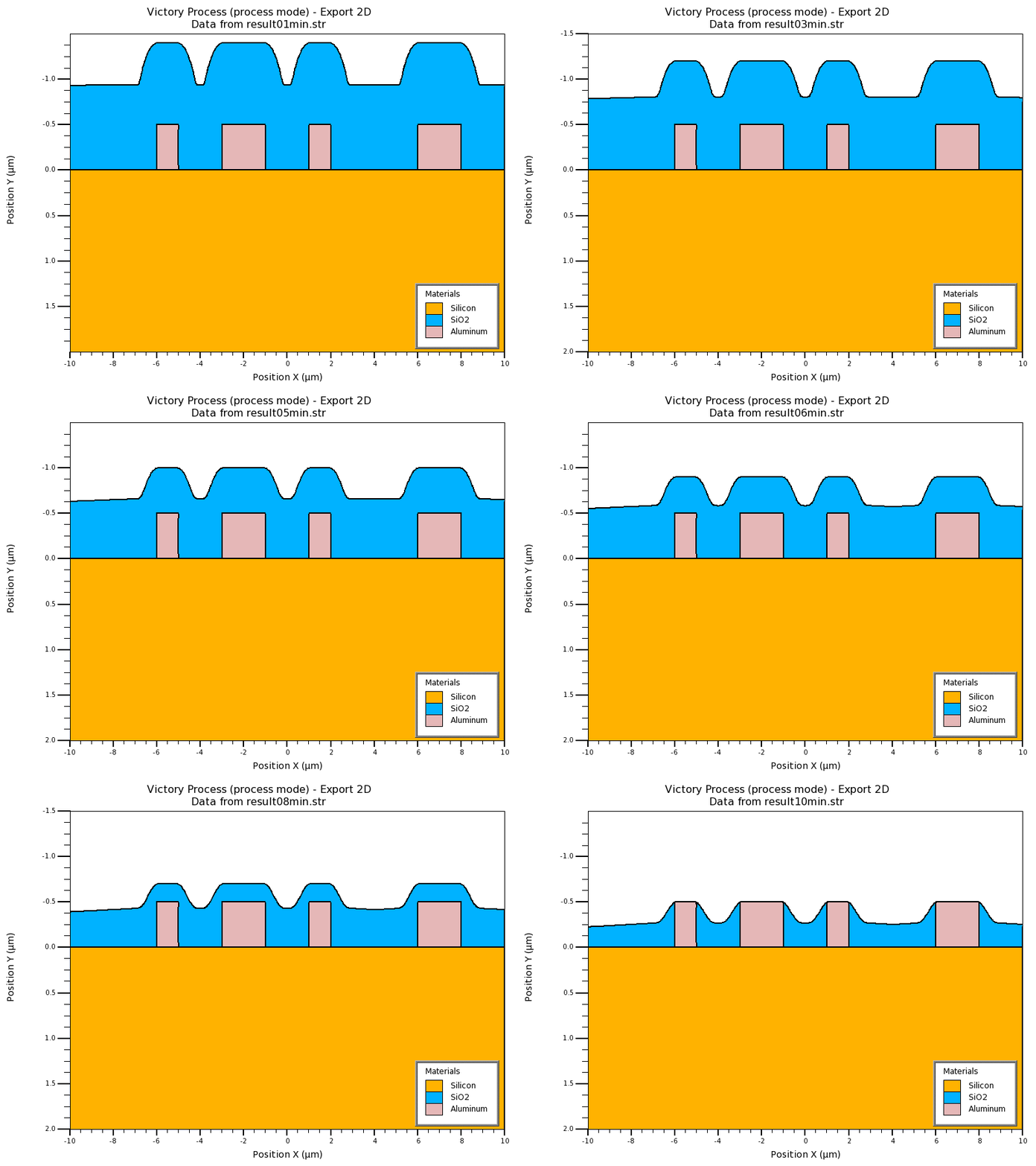
- Fast geometrical etching models for structure prototyping
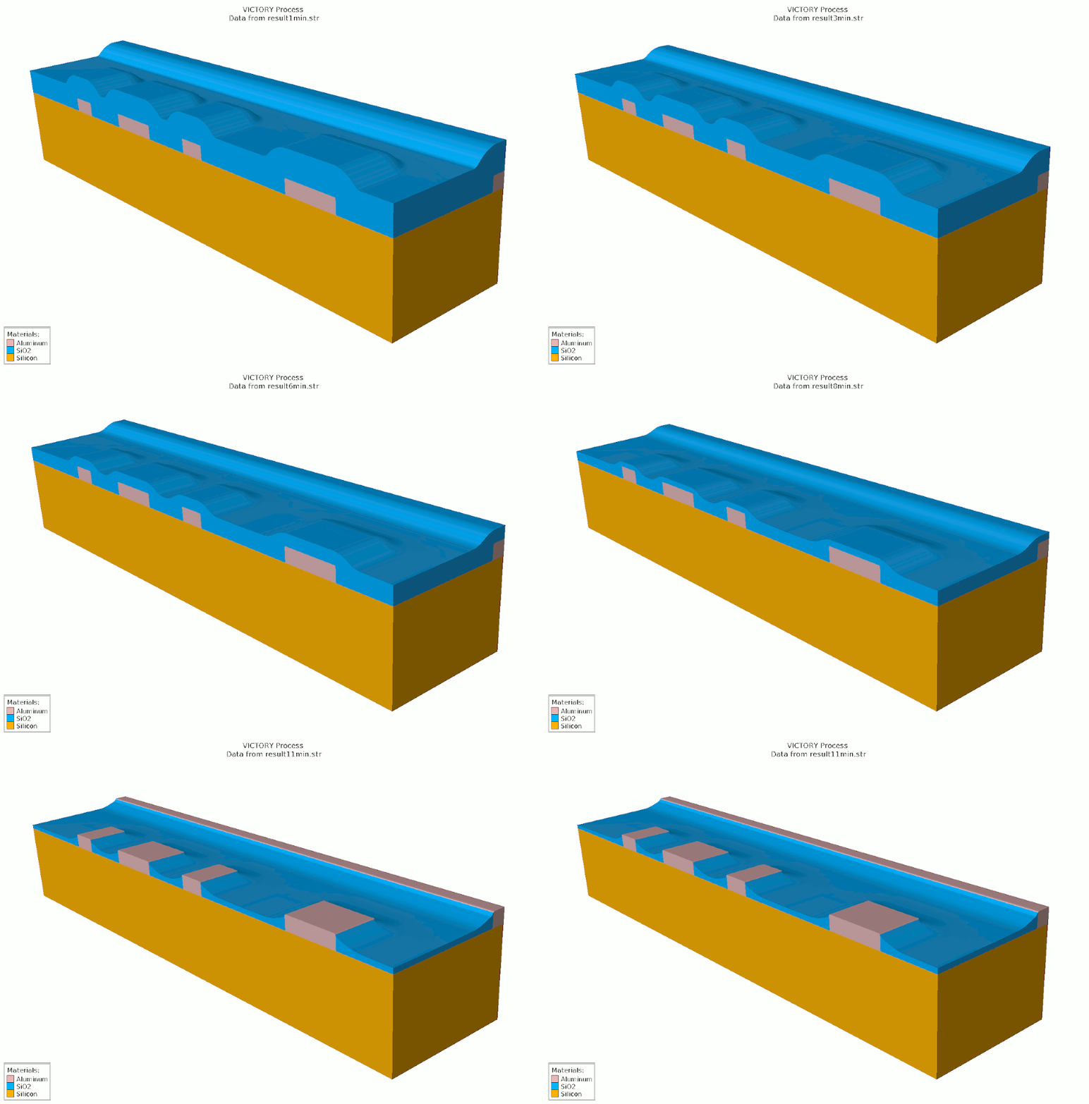
- Physical ideal wet etching with isotropic and anisotropic etching characteristics
- Idealized physical dry etching with selectivity
- Physical etching of complex multi-material structures with selectivity
- Shading and visibility effects are taken into account
- Secondary effects are taken into account including reflection of reactive particles & redeposition of extracted material
- Multi-particle physical etching models supported, for example Ion Enhanced Chemical Etch model
- Ion milling model with comprehensive beam controls, material-specific tabulated yield functions
Photolithography
- Based on GDSII layout
- Two dimensional, large numerical aperture, and aerial image formation
- Extensive source and pupil plane filtering for enhanced aerial images
- Full phase shift and transmittance variation mask capabilities
Stress & Strain
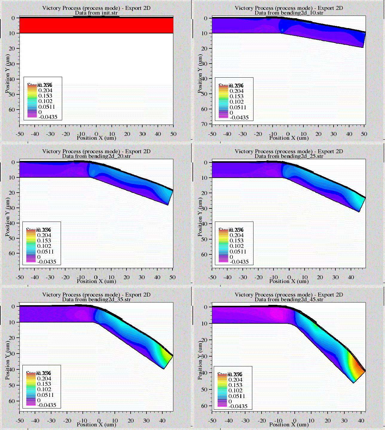
- Stress analysis during or after process simulation, on arbitrary 2D or 3D structure
- Models for various sources of strain and stress:
- Thermal mismatch between material layers
- Local lattice mismatch due to material interfaces of dissimilar materials
- Initial deposit stress in specified regions
- External (hydro-static) stress from capping layers
- Stress/strain generated in previous processing step (e.g., oxidation).
- Stress simulation for various crystalline (e.g., Si, SiGe, GaAs) materials with anisotropic stress accounting for wafer orientation, and isotropic (e.g., silicon nitride and oxide) materials.
TCAD Resources
Presentations
- Parasitic Extraction Clever and Hipex FS – Integrated Full Chip and Cell Level RCX Combine Rule Based and Field Solver Solutions
- DTCO Tool Flow – Single Run-Time Environment for Design Technology Co-Optimization
- Optical Simulations – Light Emitting and Absorbing Devices
- Power Device Solutions – Full TCAD to SPICE Flow
- Parasitic Extraction – Full Chip and Cell Level RC Extraction
- Process Simulation Options – Four Ways to Create a Physical Structure
- Radiation Effects Module – Total Dose and Single Event Phenomenon, Damage Inducing and Elastic Interactions
- Victory Atomistic – Practical Atomic-Scale Simulation
Product Briefs
Published Papers
Simulation Standard
Webinars
How to Search, View and Use Default Parameters from Silvaco Material DataBase SMDB with DeckBuild
3D TCAD Simulation of Gallium Nitride Tri-gate Junction HEMT
Writing an Impurity Activation Model with the Open Model Library
User Probes and Arbitrary Parameter Sweeps in Victory Device