Two-Dimensional Device Simulation of the InGaAs/InP Avalanche Photodiodes
1. Introduction
The high gain, and high gain-bandwidth product of the avalanche photodiodes is one of the key device for the long distance optical communication systems. For the 0.92-1.65um wavelength range, the narrow bandgap materials, like InGaAs(0.77eV), are used as the absorption medium. And the breakdown location is a major issue to design of the APD’s. In order for the device to operate with high gain and low noise[1], the design of the guard ring to suppress edge breakdown is important.
The object of this article is to get the multiplication[2], the leakage current under the dark and the illuminated current[3] was simulated. And the other important factor of the cut-off frequency calculated by the numerical device simulator ATLAS.
2. Device Structure and Models
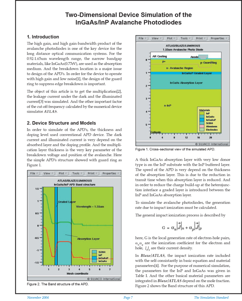
In order to simulate of the APD’s, the thickness and doping level used conventional APD device. The dark current and illuminated current is very depend on the absorbed layer and the doping profile. And the multiplication layer thickness is the very key parameter of the breakdown voltage and position of the avalanche. Here the simple APD’s structure showed with guard ring as Figure 1.


