Quantum Transport Simulation at Atomistic Accuracy of a Nanowire FET
I. ABSTRACT
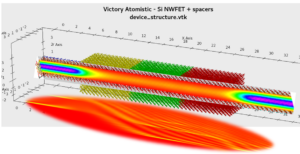 Ultra-scaled field-effect transistor (FET) technology requires simulations at the atomic scale for designing the most advanced technological architectures, at 5 nm node and below. We present in detail the Victory Atomistic solution inherited from Nemo5 [1]. Thanks to a combination of non-equilibrium Green’s functions (NEGF) and state-of-the-art band structure calculations, versatile, predictive, and fast simulations become accessible for electron-phonon interaction within the self-consistent Born approximation, optimized by a generalized low-rank projection [2]. To illustrate the Victory Atomistic usage, we choose a silicon nanowire field-effect transistor (NWFET) of small cross-section, including several e-ph scattering mechanisms. This Simulation Standard paper aims to show how simulating NWFETs becomes easy to perform without full academic knowledge of the NEGF theory: 1) the complexity is hidden inside the simulation tool which benefits from years of development at the best level, 2) its optimization allows users to obtain a meaningful I(V) curve daily with an affordable modern computer, 3) its integration within the Silvaco environment provides a smooth transition for TCAD users.
II. INTRODUCTION
The FET physical dimensions continue to shrink to five nm node and below, characterized by new types of architectures with nanosheet (NS) and nanowire (NW) shapes [3]. The present choice of material is made of Si, Ge, or SiGe alloy thanks to their high carrier concentrations. In compliment to III-V technology envisaged for a while, new 2D materials are also investigated (for example, the TMDs monolayers1). Such nanomaterials and nano-architectures require atomistic simulations for at least two crucial reasons: 1) bulk parameters like the effective masses and forbidden bandgap are no longer pertinent quantities, and 2) the wave nature of charge carriers becomes predominant for predicting transport characteristics including scattering events.
NEGF allows us to perform quantum transport simulation of such a device made of two leads and an active region, where carriers move according to a custom band structure [4]. In practice, one builds the device’s Hamiltonian on a basis of atomic wave functions and solves the coupled NEGF and Poisson equations within that basis. This comes at the price of a very high computational burden, which becomes almost untractable when scattering self-energies of inelastic carrier interactions are included [5]. Thankfully, by generalizing a low-rank approximation (LRA) with atomistic mode-space scheme [2,6], the computational load can be drastically reduced while preserving accuracy.


