3D TCAD Simulation of Gallium Nitride Tri-gate Junction HEMT
Yunwei Ma, Yuhao Zhang
Center for Power Electronics Systems, Virginia Tech
E-mail: yunwei@vt.edu; yhzhang@vt.edu
Introduction
 The GaN high electron mobility transistor (HEMT) has been commercialized as a power device with performance superior to Si devices in the voltage classes from 15 V to 900 V [1]. Most of commercial enhancement-mode (E-mode) HEMTs comprise a planar p-GaN gate. Recently, 3-D gate stacks, such as FinFET and tri-gate structures, have been introduced to lateral GaN HEMTs. They can realize superior gate controllability and E-mode operation with a higher current on/off ratio and lower gated channel resistance [2].
On each facet of the tri-gate, the metal-insulator-semiconductor (MIS) gate stack has become a popular choice [3]. Despite good performance, some challenges of tri-gate GaN MIS-HEMTs (Tri-MISHEMTs) make their commercialization very slow. First, the E-mode device usually requires very narrow fins or an additional AlGaN recess [2]. Second, the MIS tri-gate produces parasitic MIS channels at the fin sidewalls, which increase the gate charge. In addition, the commonly seen interface states in the MIS structure could induce high-temperature instabilities [4].
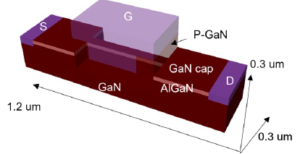
To address these challenges, we recently proposed a new type of tri-gate HEMTs, the tri-gate junction HEMT (Tri-JHEMT) [5]. In the Tri-JHEMT, the p-n junction wraps around the AlGaN/GaN fins in the gate region. As compared to the MIS tri-gate, the junction tri-gate allows stronger depletion, thus relaxing the lithography requirement to realize the E-mode operation and avoiding the punch-through at high drain biases (VD) [5]. A GaN Tri-JHEMT is then experimentally demonstrated using the p-type NiO [5], which exhibits the E-mode operation, high breakdown voltage, and excellent thermal stability (e.g., a breakdown voltage near 2000 V at 150 oC) [6].
Following the experimental demonstration, we studied the physics and performance space of Tri-JHEMTs using the 3D TCAD simulation [7]. In this study, we used the NiO-based Tri-JHEMT data to calibrate the 3D TCAD simulation model, followed by the simulation of p-GaN based Tri-JHEMT. The p-GaN based junction tri-gate is expected to provide a stronger depletion as compared to the NiO-based tri-gate, due to the higher built-in potential of the GaN p-n junction as compared to the GaN/NiO junction. In addition, the p-GaN based Tri-JHEMT can be potentially fabricated using the current foundry process. 3D TCAD simulations enable a direct comparison of the Tri-JHEMT with the planar p-GaN HEMT.
This article describes the 3D TCAD simulation of GaN trigate HEMTs and showcases how 3D simulations unveil the Tri-JHEMT’s unique physics as compared to the planar-gate HEMT or Tri-MISHEMT.


