Simulation Standard
Technical Journal
A Journal for Process and Device Engineers
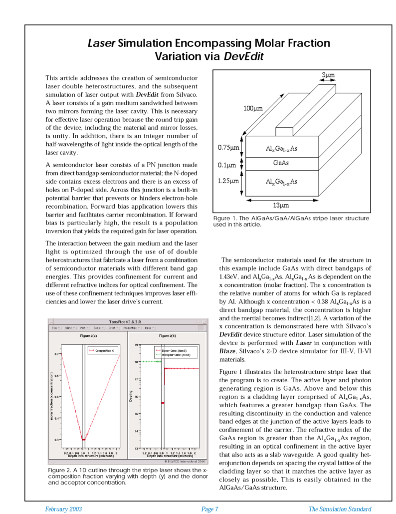
Laser Simulation Encompassing Molar Fraction Variation via DevEdit
This article addresses the creation of semiconductor laser double heterostructures, and the subsequent simulation of laser output with DevEdit from Silvaco. A laser consists of a gain medium sandwiched between two mirrors forming the laser cavity. This is necessary for effective laser operation because the round trip gain of the device, including the material and mirror losses, is unity. In addition, there is an integer number of half-wavelengths of light inside the optical length of the laser cavity.
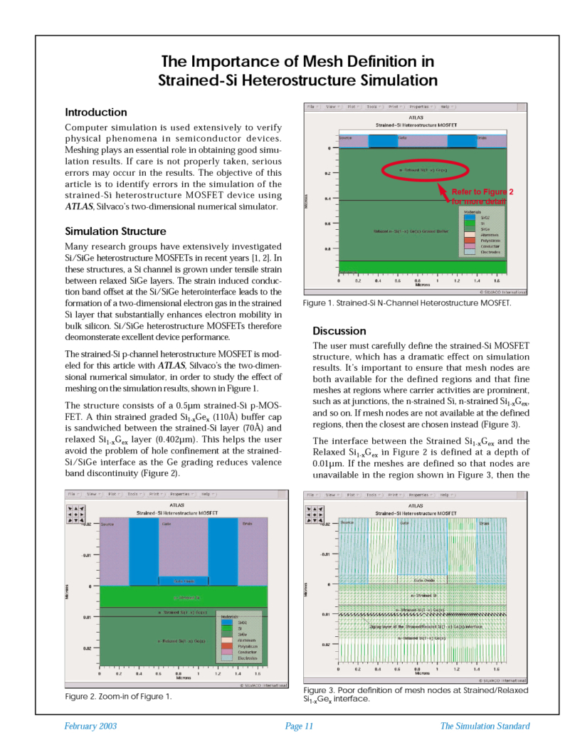
The Importance of Mesh Definition in Strained-Si Heterostructure Simulation
Computer simulation is used extensively to verify physical phenomena in semiconductor devices. Meshing plays an essential role in obtaining good simulation results. If care is not properly taken, serious errors may occur in the results. The objective of this article is to identify errors in the simulation of the strained-Si heterostructure MOSFET device using ATLAS, Silvaco’s two-dimensional numerical simulator.
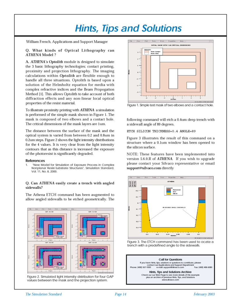
Optical Lithography Models in ATHENA
ATHENA’s Optolith module is designed to simulate the 3 basic lithography technologies; contact printing, proximity and projection lithography. The imaging calculations within Optolith are flexible enough to handle all three situations. Optolith is based upon a solution of the Helmholtz equation for media with complex refractive indices and the Beam Propogation Method [1]. This allows Optolith to take account of both diffraction effects and any non-linear local optical properties of the resist material.
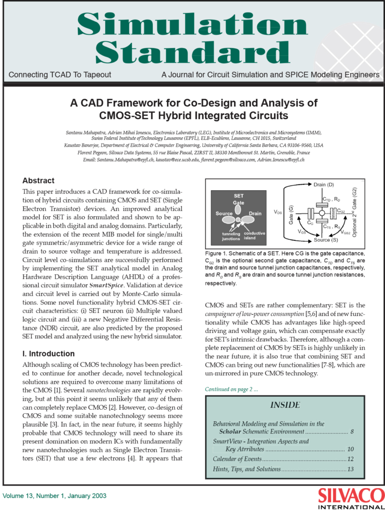
A CAD Framework for Co-Design and Analysis of CMOS-SET Hybrid Integrated Circuits
This paper introduces a CAD framework for co-simulation of hybrid circuits containing CMOS and SET (Single Electron Transistor) devices. An improved analytical model for SET is also formulated and shown to be applicable in both digital and analog domains.
Behavioral Modeling and Simulation in the Scholar Schematic Environment
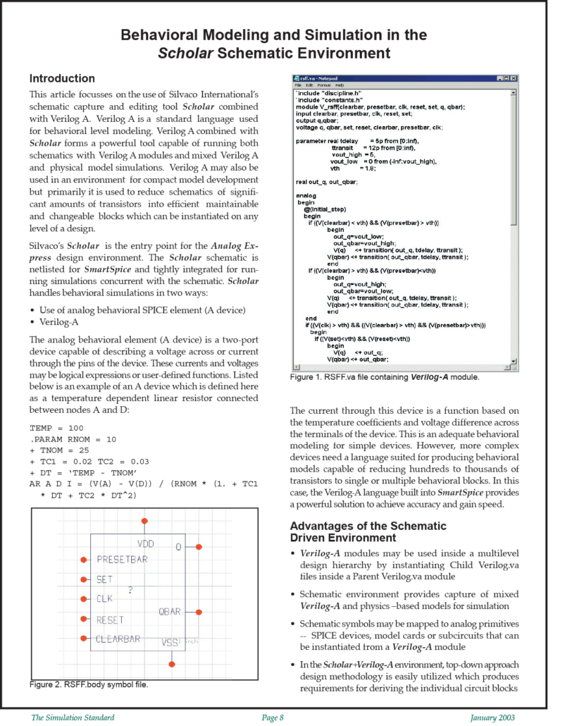
This article focusses on the use of Silvaco International’s schematic capture and editing tool Scholar combined with Verilog A. Verilog A is a standard language used for behavioral level modeling. Verilog A combined with Scholar forms a powerful tool capable of running both schematics with Verilog A modules and mixed Verilog A and physical model simulations. Verilog A may also be used in an environment for compact model development but primarily it is used to reduce schematics of significant amounts of transistors into efficient maintainable and changeable blocks which can be instantiated on any level of a design.
SmartView – Integration Aspects and Key Attributes
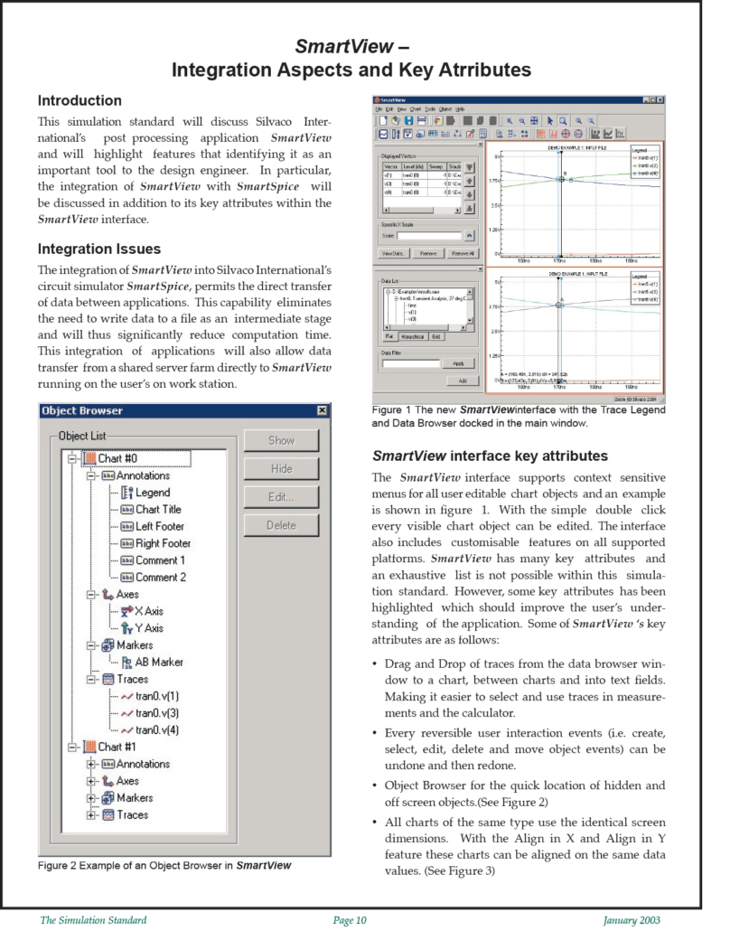
This simulation standard will discuss Silvaco International’s post processing application SmartView and will highlight features that identifying it as an important tool to the design engineer. In particular, the integration of SmartView with SmartSpice will be discussed in addition to its key attributes within the SmartView interface.

