Simulation Standard
Technical Journal
A Journal for Process and Device Engineers
Using VICTORY Process to Model Thermal Oxidation of Silicon in O2/HCl Mixtures
The addition of a chlorine species during thermal oxidation of silicon results in improved threshold stability, higher and more uniform oxide dielectric strength and improved junction properties due to lower leakage [1-3]. The effect of HCl addition is to increase the oxidation rate relative to the oxidation rate in dry oxidation ambient (O2), whilst no influence of HCL on the oxidation rate is seen for wet oxidation ambient (H20). The observed increase in oxidation rate is due to:
Thermal Optimization on GaN HFET Using Flip Chip and Through Wafer via Structures
GaN heterojunction field effect transistors (HFETs) have been under extensive investigation because of their projected superb performances as high-power RF devices. The inherently high breakdown field arising from the wide bandgap guarantees not only the high power input/output characteristics but also extreme device shrinkage which is a huge advantage for increasing the highest operation frequency. Two-dimensional electron gas (2-DEG) with the charge density ten times higher than that of GaAs-based HFET and the mobility well exceeding Si enables a very low on-state resistance indispensable to RF devices. Although the superiority of the device characteristics has been demonstrated, the self heating effect has hindered the production of high power and high speed GaN-based switching devices. This effect can be significantly reduced by the cost effective heat-sink approach (Flip chip or through wafer via)[1,2].
3D Simulation of Ion Enhanced Chemical Etching with VICTORY Process
VICTORY Process is a tool for 3D simulation of the semiconductor industry’s technological processes. It allows stable and accurate modeling of the changes in a structure’s 3D geometry within etching reactors under various conditions. VICTORY Process achieves this by combining a powerful and robust hard-coded numerical engine, based on the Level Set method, with a flexible Open Modeling library which is extendable by users to suit their specific requirements.
Simulation of Transient Diffusion Enhancement of Boron with VICTORY Process in 3D, with the Plus-One Implantation Damage Model and the Five-Stream Diffusion Model
VICTORY Process is a 3D process simulation tool which allows for an accurate simulation of the doping distributions in semiconductor devices. It is able to simulate both the insertion of the doping atoms by ion implantation and their subsequent redistribution by thermal treatment.
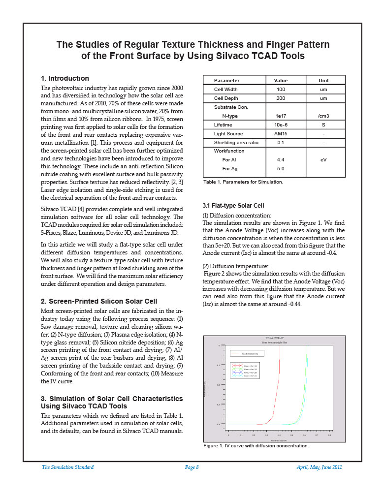
The Studies of Regular Texture Thickness and Finger Pattern of the Front Surface by Using Silvaco TCAD Tools
The photovoltaic industry has rapidly grown since 2000 and has diversified in technology how the solar cell are manufactured. As of 2010, 70% of these cells were made from mono- and multicrystalline silicon wafer, 20% from thin films and 10% from silicon ribbons. In 1975, screen printing was first applied to solar cells for the formation of the front and rear contacts replacing expensive vacuum metallization [1]. This process and equipment for the screen-printed solar cell has been further optimized and new technologies have been introduced to improve this technology. These include an anti-reflection Silicon nitride coating with excellent surface and bulk passivity properties. Surface texture has reduced reflectivity. [2, 3] Laser edge isolation and single-side etching is used for the electrical separation of the front and rear contacts.
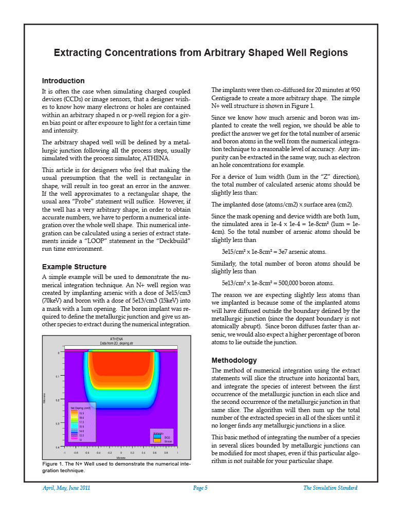
Extracting Concentrations from Arbitrary Shaped Well Regions
It is often the case when simulating charged coupled devices (CCDs) or image sensors, that a designer wishes to know how many electrons or holes are contained within an arbitrary shaped n or p-well region for a given bias point or after exposure to light for a certain time and intensity.

