Simulation Framework for Device-packaging Co-design for Power Electronics
Introduction
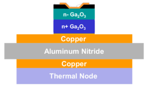 The past several years has seen a fast deployment of wide-bandgap power devices in fast chargers, electric vehicles, data centers and renewable energy processing. The performance of power devices is fast progressing towards their intrinsic material limit. As these devices can handle higher voltage and larger current density, packaging and thermal management will become the key limiting factor for exploiting their benefits in power electronic converters and systems. Due to the diversity of power devices (e.g., different layout, channel locations, hot spot distributions), there would be no packaging solution universally optimal for all power devices. Hence, device-packaging co-design is essential. However, the large dimension range (from nm in devices to mm in packaging) makes it difficult to realize precise and time-efficient physical simulations. Conventional finite element analysis (FEA) tools, can enable relatively fast simulations for packaging structures but cannot do the self-consistent electrothermal simulation for devices. In this work, we explore the integration of device TCAD simulations and packaging FEA, with the goal of building up a precise and time-efficient simulation framework for device-packaging co-design.


