The Importance of Mesh Definition in Strained-Si Heterostructure Simulation
Introduction
Computer simulation is used extensively to verify physical phenomena in semiconductor devices. Meshing plays an essential role in obtaining good simulation results. If care is not properly taken, serious errors may occur in the results. The objective of this article is to identify errors in the simulation of the strained-Si heterostructure MOSFET device using ATLAS, Silvaco’s two-dimensional numerical simulator.
Simulation Structure
Many research groups have extensively investigated Si/SiGe heterostructure MOSFETs in recent years [1, 2]. In these structures, a Si channel is grown under tensile strain between relaxed SiGe layers. The strain induced conduction band offset at the Si/SiGe heterointerface leads to the formation of a two-dimensional electron gas in the strained Si layer that substantially enhances electron mobility in bulk silicon. Si/SiGe heterostructure MOSFETs therefore deomonsterate excellent device performance.
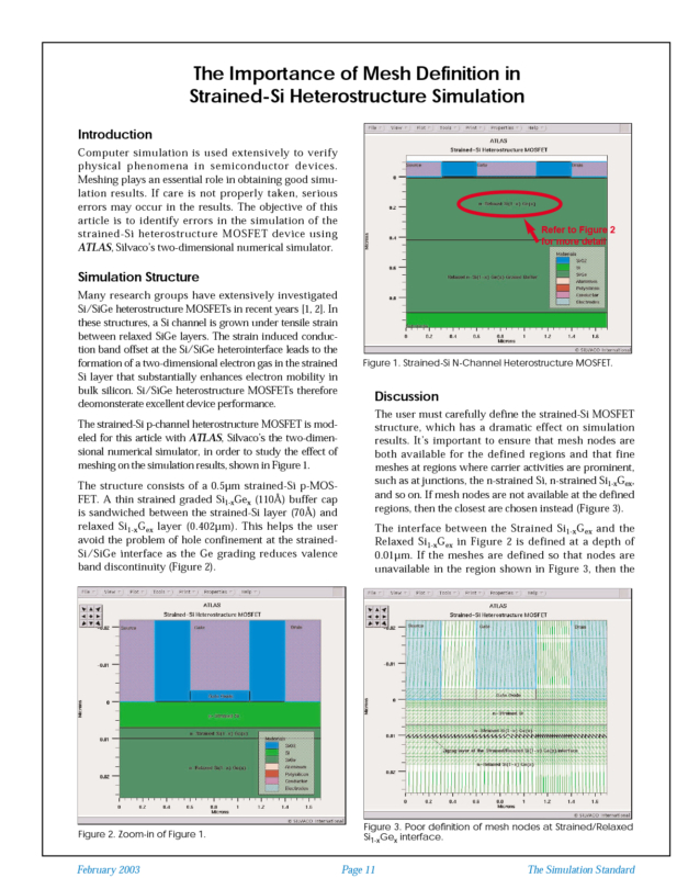
The strained-Si p-channel heterostructure MOSFET is modeled for this article with ATLAS, Silvaco’s the two-dimensional numerical simulator, in order to study the effect of meshing on the simulation results, shown in Figure 1.
The structure consists of a 0.5µm strained-Si p-MOSFET. A thin strained graded Si1-xGex (110Å) buffer cap is sandwiched between the strained-Si layer (70Å) and relaxed Si1-xGex layer (0.402µm). This helps the user avoid the problem of hole confinement at the strained-Si/SiGe interface as the Ge grading reduces valence band discontinuity (Figure 2).


