 https://silvaco.com/wp-content/uploads/2020/02/RFSOI-trap_fig3.jpg
417
550
Erick Castellon
/wp-content/uploads/2019/11/silvaco-logo.png
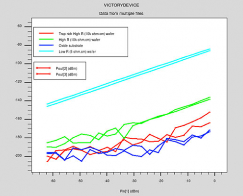
Erick Castellon2019-09-03 00:00:252021-07-16 21:34:48RFSOI Switch Harmonics Simulations with Trap-Rich Substrate
https://silvaco.com/wp-content/uploads/2020/02/RFSOI-trap_fig3.jpg
417
550
Erick Castellon
/wp-content/uploads/2019/11/silvaco-logo.png
Erick Castellon2019-09-03 00:00:252021-07-16 21:34:48RFSOI Switch Harmonics Simulations with Trap-Rich Substrate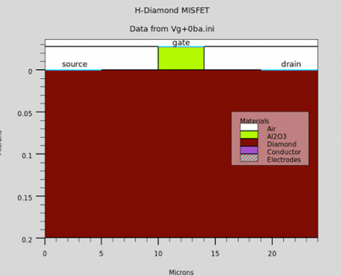 https://silvaco.com/wp-content/uploads/2020/02/diamond_fig1.jpg
428
550
Erick Castellon
/wp-content/uploads/2019/11/silvaco-logo.png
Erick Castellon2019-09-03 00:00:032021-07-16 21:34:48Estimation of Interface Property Changes Between Normally On/Off Hydrogenated Diamond MISFETs
https://silvaco.com/wp-content/uploads/2020/02/diamond_fig1.jpg
428
550
Erick Castellon
/wp-content/uploads/2019/11/silvaco-logo.png
Erick Castellon2019-09-03 00:00:032021-07-16 21:34:48Estimation of Interface Property Changes Between Normally On/Off Hydrogenated Diamond MISFETs https://silvaco.com/wp-content/uploads/2019/07/VT_fig2.jpg
283
401
Erick Castellon
/wp-content/uploads/2019/11/silvaco-logo.png
Erick Castellon2019-07-05 00:00:502021-07-16 21:34:48TCAD Simulation of Electric Field Distribution in Gallium Nitride Trench-based Power Devices
https://silvaco.com/wp-content/uploads/2019/07/VT_fig2.jpg
283
401
Erick Castellon
/wp-content/uploads/2019/11/silvaco-logo.png
Erick Castellon2019-07-05 00:00:502021-07-16 21:34:48TCAD Simulation of Electric Field Distribution in Gallium Nitride Trench-based Power Devices https://silvaco.com/wp-content/uploads/2020/02/ss_self-heating_fig1.jpg
397
550
Erick Castellon
/wp-content/uploads/2019/11/silvaco-logo.png
Erick Castellon2019-07-04 00:00:192021-07-16 21:34:49Channel-length Dependence of a-IGZO TFTs with Self-heating Effects
https://silvaco.com/wp-content/uploads/2020/02/ss_self-heating_fig1.jpg
397
550
Erick Castellon
/wp-content/uploads/2019/11/silvaco-logo.png
Erick Castellon2019-07-04 00:00:192021-07-16 21:34:49Channel-length Dependence of a-IGZO TFTs with Self-heating Effects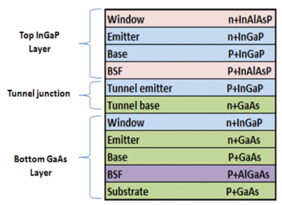 https://silvaco.com/wp-content/uploads/2020/02/solar_cell_fig2.jpg
299
411
Erick Castellon
/wp-content/uploads/2019/11/silvaco-logo.png
Erick Castellon2019-07-03 00:00:592021-07-16 21:34:49Simulation of Different Tunnel Junctions in InGaP/GaAs, InGaP/CdTe Dual Junction Solar Cells
https://silvaco.com/wp-content/uploads/2020/02/solar_cell_fig2.jpg
299
411
Erick Castellon
/wp-content/uploads/2019/11/silvaco-logo.png
Erick Castellon2019-07-03 00:00:592021-07-16 21:34:49Simulation of Different Tunnel Junctions in InGaP/GaAs, InGaP/CdTe Dual Junction Solar Cells https://silvaco.com/wp-content/uploads/2019/07/hts-July-2019-thumb.png
875
900
Erick Castellon
/wp-content/uploads/2019/11/silvaco-logo.png
Erick Castellon2019-07-01 22:50:502021-07-16 21:35:03Hints, Tips and Solutions – July, August, September 2019
https://silvaco.com/wp-content/uploads/2019/07/hts-July-2019-thumb.png
875
900
Erick Castellon
/wp-content/uploads/2019/11/silvaco-logo.png
Erick Castellon2019-07-01 22:50:502021-07-16 21:35:03Hints, Tips and Solutions – July, August, September 2019 https://silvaco.com/wp-content/uploads/2019/04/VP_fig5.jpg
471
550
Erick Castellon
/wp-content/uploads/2019/11/silvaco-logo.png
Erick Castellon2019-04-01 10:00:342021-07-16 21:35:04Process Simulation – New Features in 2019 Baseline Release
https://silvaco.com/wp-content/uploads/2019/04/VP_fig5.jpg
471
550
Erick Castellon
/wp-content/uploads/2019/11/silvaco-logo.png
Erick Castellon2019-04-01 10:00:342021-07-16 21:35:04Process Simulation – New Features in 2019 Baseline Release https://silvaco.com/wp-content/uploads/2020/03/fig11.jpg
469
550
Erick Castellon
/wp-content/uploads/2019/11/silvaco-logo.png
Erick Castellon2019-04-01 09:00:112021-07-16 21:35:04Meshing – New Features in 2019 Baseline Release
https://silvaco.com/wp-content/uploads/2020/03/fig11.jpg
469
550
Erick Castellon
/wp-content/uploads/2019/11/silvaco-logo.png
Erick Castellon2019-04-01 09:00:112021-07-16 21:35:04Meshing – New Features in 2019 Baseline Release https://silvaco.com/wp-content/uploads/2019/04/device_fig2-6b.jpg
312
312
Erick Castellon
/wp-content/uploads/2019/11/silvaco-logo.png
Erick Castellon2019-04-01 08:00:192021-07-16 21:35:05Device Simulation – New Features in 2019 Baseline Release
https://silvaco.com/wp-content/uploads/2019/04/device_fig2-6b.jpg
312
312
Erick Castellon
/wp-content/uploads/2019/11/silvaco-logo.png
Erick Castellon2019-04-01 08:00:192021-07-16 21:35:05Device Simulation – New Features in 2019 Baseline Release https://silvaco.com/wp-content/uploads/2020/03/DB_fig4-6.jpg
425
550
Erick Castellon
/wp-content/uploads/2019/11/silvaco-logo.png
Erick Castellon2019-04-01 07:00:592021-07-16 21:35:05Interactive Tools – New Features in 2019 Baseline Release
https://silvaco.com/wp-content/uploads/2020/03/DB_fig4-6.jpg
425
550
Erick Castellon
/wp-content/uploads/2019/11/silvaco-logo.png
Erick Castellon2019-04-01 07:00:592021-07-16 21:35:05Interactive Tools – New Features in 2019 Baseline Release