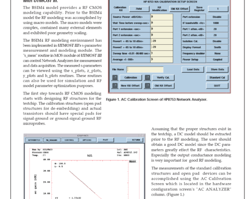
BSIM4 RF CMOS Modeling with UTMOST III
The BSIM4 model provides a RF CMOS modeling capability. Prior to the BSIM4 model the RF modeling was accomplished by using macro models. The macro models were complex, contained many external elements and exhibited poor geometry scaling.
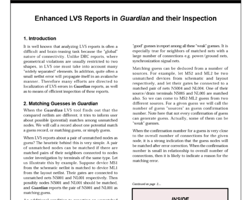
Enhanced LVS Reports in Guardian and Their Inspection
It is well known that analyzing LVS reports is often a difficult and brain-teasing task because the "global" nature of connectivity. Unlike DRC reports, where geometrical violations are usually restricted to two shapes, in LVS one must take into account many "widely separated" elements. In addition, quite often a small netlist error will propagate itself in an avalanche manner. Therefore many efforts are directed to localization of LVS errors in Guardian reports, as well as to means of efficient inspection of these reports.
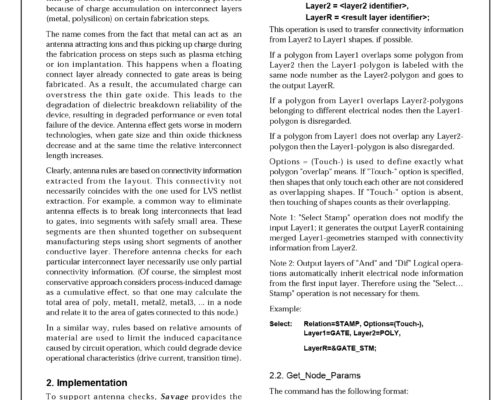
Antenna Rule Checks in Savage
Antenna rules is a common name for rules that check ratios of amounts of material in two layers from the same node. They are used to limit the damage of the thin gate oxide during the manufacturing process because of charge accumulation on interconnect layers (metal, polysilicon) on certain fabrication steps.
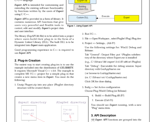
Expert’s Application Programming Interface (Expert API)
Expert API is intended for customizing and extending the existing software functionality by functions written by the users of Expert using C/C++.
Add Custom Commands to Expert’s Menu
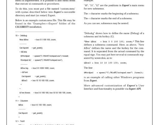
A simple way to add custom commands to Expert's menu is implemented. It is possible to add menu items that execute xi-commands or procedures. To do this, you must put a file named 'custom.mnu' with syntax described below into Expert's executable directory and start (or restart) Expert.
Non-Stationary Transport Effects: Impact on Performances of Realistic 50nm MOSFET Technology
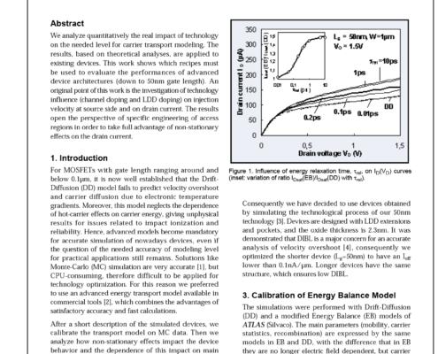
We analyze quantitatively the real impact of technology on the needed level for carrier transport modeling. The results, based on theoretical analyses, are applied to existing devices. This work shows which recipes must be used to evaluate the performances of advanced device architectures (down to 50nm gate length).
QUEST: Frequency-Dependent RLCG Extractor
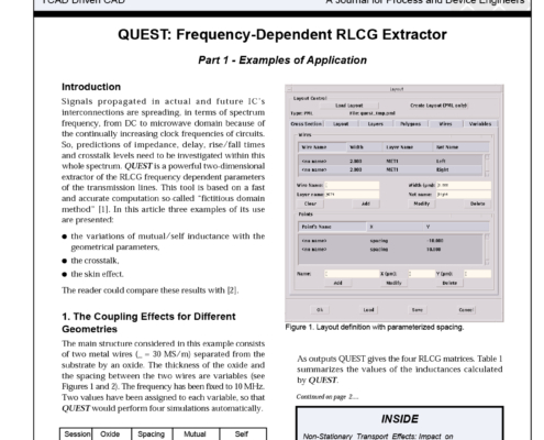
Signals propagated in actual and future IC's interconnections are spreading, in terms of spectrum frequency, from DC to microwave domain because of the continually increasing clock frequencies of circuits. So, predictions of impedance, delay, rise/fall times and crosstalk levels need to be investigated within this whole spectrum. QUEST is a powerful two-dimensional extractor of the RLCG frequency dependent parameters of the transmission lines.
Modeling of Charge Distribution Using Schrodinger-Poisson Equations: Application to Double-Gate GAA-SOI Transistor
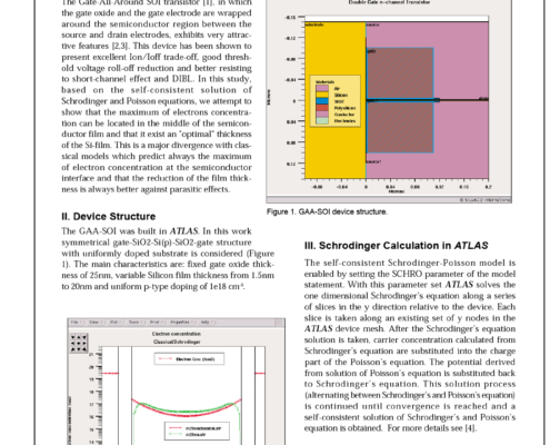
The Gate-All-Around SOI transistor [1], in which the gate oxide and the gate electrode are wrapped around the semiconductor region between the source and drain electrodes, exhibits very attractive features [2,3]. This device has been shown to present excellent Ion/Ioff trade-off, good threshold voltage roll-off reduction and better resisting to short-channel effect and DIBL. In this study, based on the self-consistent solution of Schrodinger and Poisson equations, we attempt to show that the maximum of electrons concentration can be located in the middle of the semiconductor film and that there exists
an "optimal" thickness of the Si-film.
 https://silvaco.com/wp-content/uploads/simulationstandard/simstd_feb_2002_hints.jpg
1669
1287
Graham Bell
/wp-content/uploads/2019/11/silvaco-logo.png
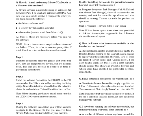
Graham Bell2002-02-01 20:15:052021-07-16 22:05:41Installing and using Silvaco TCAD tools on a Windows 2000 Machine
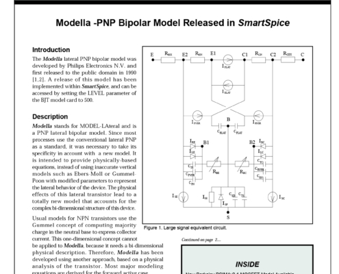
Modella PNP Bipolar Model Released in SmartSpice
The Modella lateral PNP bipolar model was developed by Philips Electronics N.V. and first released to the public domain in 1990 [1,2]. A release of this model has been implemented within SmartSpice, and can be accessed by setting the LEVEL parameter of the BJT model card to 500.
