 https://silvaco.com/wp-content/uploads/simulationstandard/simstd_jun_2003_a5-e1611193467389.jpg
800
644
Graham Bell
/wp-content/uploads/2019/11/silvaco-logo.png
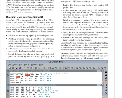
Graham Bell2003-06-01 19:12:322021-07-16 21:59:17Guardian LVS: New Platform-Independent GUI
https://silvaco.com/wp-content/uploads/simulationstandard/simstd_jun_2003_a5-e1611193467389.jpg
800
644
Graham Bell
/wp-content/uploads/2019/11/silvaco-logo.png
Graham Bell2003-06-01 19:12:322021-07-16 21:59:17Guardian LVS: New Platform-Independent GUI https://silvaco.com/wp-content/uploads/simulationstandard/simstd_jun_2003_hints.jpg
1669
1344
Graham Bell
/wp-content/uploads/2019/11/silvaco-logo.png
Graham Bell2003-06-01 18:16:002021-07-16 21:59:18Counting Instances in an Expert Editor Layout
https://silvaco.com/wp-content/uploads/simulationstandard/simstd_jun_2003_hints.jpg
1669
1344
Graham Bell
/wp-content/uploads/2019/11/silvaco-logo.png
Graham Bell2003-06-01 18:16:002021-07-16 21:59:18Counting Instances in an Expert Editor Layout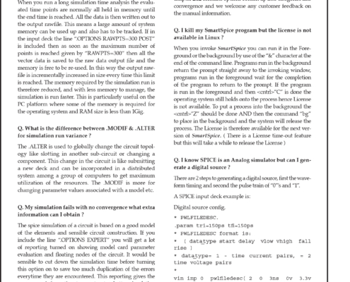 /wp-content/uploads/2019/11/silvaco-logo.png
0
0
Graham Bell
/wp-content/uploads/2019/11/silvaco-logo.png
Graham Bell2003-05-01 23:58:502021-07-16 21:59:32Low Voltage Super Junction MOSFET Simulation and Experimentation
/wp-content/uploads/2019/11/silvaco-logo.png
0
0
Graham Bell
/wp-content/uploads/2019/11/silvaco-logo.png
Graham Bell2003-05-01 23:58:502021-07-16 21:59:32Low Voltage Super Junction MOSFET Simulation and Experimentation https://silvaco.com/wp-content/uploads/simulationstandard/simstd_may_2003_a2-e1611193932945.jpg
800
644
Graham Bell
/wp-content/uploads/2019/11/silvaco-logo.png
Graham Bell2003-05-01 22:01:452021-07-16 21:59:32Using The Statistical Sampling Feature in the BCA Monte Carlo Implant Simulator
https://silvaco.com/wp-content/uploads/simulationstandard/simstd_may_2003_a2-e1611193932945.jpg
800
644
Graham Bell
/wp-content/uploads/2019/11/silvaco-logo.png
Graham Bell2003-05-01 22:01:452021-07-16 21:59:32Using The Statistical Sampling Feature in the BCA Monte Carlo Implant Simulator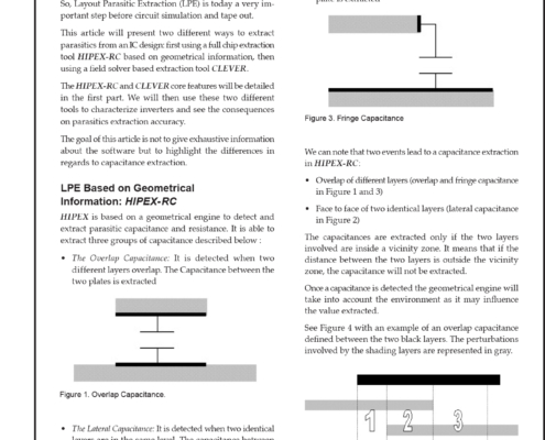 https://silvaco.com/wp-content/uploads/simulationstandard/simstd_may_2003_a3.jpg
1669
1344
Graham Bell
/wp-content/uploads/2019/11/silvaco-logo.png
Graham Bell2003-05-01 21:06:272021-07-16 21:59:33A Comparison Between Classical Full Chip Extraction and Field Solver Parasitic Extraction
https://silvaco.com/wp-content/uploads/simulationstandard/simstd_may_2003_a3.jpg
1669
1344
Graham Bell
/wp-content/uploads/2019/11/silvaco-logo.png
Graham Bell2003-05-01 21:06:272021-07-16 21:59:33A Comparison Between Classical Full Chip Extraction and Field Solver Parasitic Extraction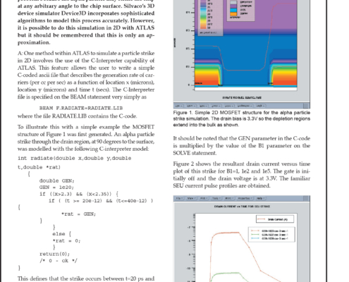 https://silvaco.com/wp-content/uploads/simulationstandard/simstd_may_2003_hints.jpg
1669
1344
Graham Bell
/wp-content/uploads/2019/11/silvaco-logo.png
Graham Bell2003-05-01 20:12:302021-07-16 21:59:33ATLAS Simulation of an SEU Event in 2D
https://silvaco.com/wp-content/uploads/simulationstandard/simstd_may_2003_hints.jpg
1669
1344
Graham Bell
/wp-content/uploads/2019/11/silvaco-logo.png
Graham Bell2003-05-01 20:12:302021-07-16 21:59:33ATLAS Simulation of an SEU Event in 2D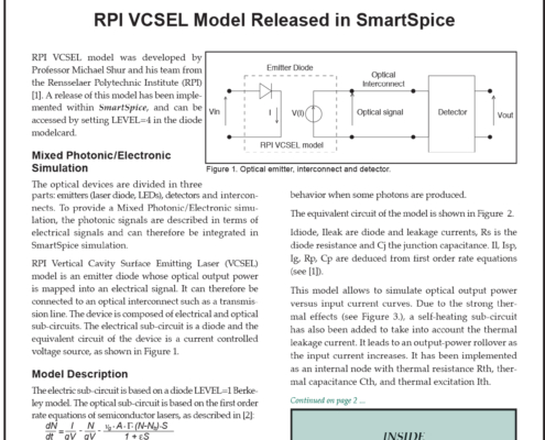 https://silvaco.com/wp-content/uploads/simulationstandard/simstd_apr_2003_a1.jpg
1669
1252
Graham Bell
/wp-content/uploads/2019/11/silvaco-logo.png
Graham Bell2003-04-01 23:54:352021-07-16 21:59:34RPI VCSEL Model Released in SmartSpice
https://silvaco.com/wp-content/uploads/simulationstandard/simstd_apr_2003_a1.jpg
1669
1252
Graham Bell
/wp-content/uploads/2019/11/silvaco-logo.png
Graham Bell2003-04-01 23:54:352021-07-16 21:59:34RPI VCSEL Model Released in SmartSpice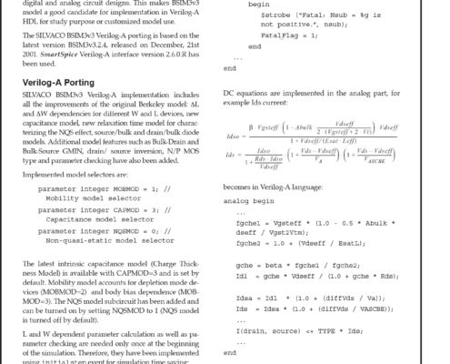 https://silvaco.com/wp-content/uploads/simulationstandard/simstd_apr_2003_a2.jpg
1669
1344
Graham Bell
/wp-content/uploads/2019/11/silvaco-logo.png
Graham Bell2003-04-01 22:58:092021-07-16 22:00:07BSIM3v3 Model Verilog-A Implementation
https://silvaco.com/wp-content/uploads/simulationstandard/simstd_apr_2003_a2.jpg
1669
1344
Graham Bell
/wp-content/uploads/2019/11/silvaco-logo.png
Graham Bell2003-04-01 22:58:092021-07-16 22:00:07BSIM3v3 Model Verilog-A Implementation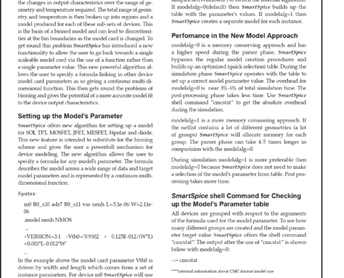 https://silvaco.com/wp-content/uploads/simulationstandard/simstd_apr_2003_a3-e1611191887574.jpg
1000
805
Graham Bell
/wp-content/uploads/2019/11/silvaco-logo.png
Graham Bell2003-04-01 21:01:422021-07-16 22:00:08New Device Model Card Approach
https://silvaco.com/wp-content/uploads/simulationstandard/simstd_apr_2003_hints-e1611194237217.jpg
800
644
Graham Bell
/wp-content/uploads/2019/11/silvaco-logo.png
Graham Bell2003-04-01 19:06:232021-07-16 22:00:08SmartSpice Tips: Memory Usage, .MODIF & .ALTER, Non-convergence
https://silvaco.com/wp-content/uploads/simulationstandard/simstd_apr_2003_a3-e1611191887574.jpg
1000
805
Graham Bell
/wp-content/uploads/2019/11/silvaco-logo.png
Graham Bell2003-04-01 21:01:422021-07-16 22:00:08New Device Model Card Approach
https://silvaco.com/wp-content/uploads/simulationstandard/simstd_apr_2003_hints-e1611194237217.jpg
800
644
Graham Bell
/wp-content/uploads/2019/11/silvaco-logo.png
Graham Bell2003-04-01 19:06:232021-07-16 22:00:08SmartSpice Tips: Memory Usage, .MODIF & .ALTER, Non-convergence