 https://silvaco.com/wp-content/uploads/2020/03/simstd_Q3_2014_hints1.jpg
1012
782
Ingrid Schwarz
/wp-content/uploads/2019/11/silvaco-logo.png
Ingrid Schwarz2014-07-01 16:02:242021-07-16 21:40:58Hints, Tips and Solutions – Meshing a Non Axis Aligned SEU Beam
https://silvaco.com/wp-content/uploads/2020/03/simstd_Q3_2014_hints1.jpg
1012
782
Ingrid Schwarz
/wp-content/uploads/2019/11/silvaco-logo.png
Ingrid Schwarz2014-07-01 16:02:242021-07-16 21:40:58Hints, Tips and Solutions – Meshing a Non Axis Aligned SEU Beam https://silvaco.com/wp-content/uploads/2020/03/simstd_Q2_2014_hints2.jpg
1012
782
Ingrid Schwarz
/wp-content/uploads/2019/11/silvaco-logo.png
Ingrid Schwarz2014-04-01 19:41:272021-07-16 21:40:58Hints, Tips, and Solutions – Calculate Light Extraction Efficiency in an OLED or LED with Pure Optical Simulation
https://silvaco.com/wp-content/uploads/2020/03/simstd_Q2_2014_hints2.jpg
1012
782
Ingrid Schwarz
/wp-content/uploads/2019/11/silvaco-logo.png
Ingrid Schwarz2014-04-01 19:41:272021-07-16 21:40:58Hints, Tips, and Solutions – Calculate Light Extraction Efficiency in an OLED or LED with Pure Optical Simulation https://silvaco.com/wp-content/uploads/2020/03/simstd_Q2_2014_hints1.jpg
1012
782
Ingrid Schwarz
/wp-content/uploads/2019/11/silvaco-logo.png
Ingrid Schwarz2014-04-01 19:34:052021-07-16 21:41:12Hints, Tips, and Solutions – Achieve Publication Quality Plots Using TonyPlot
https://silvaco.com/wp-content/uploads/2020/03/simstd_Q2_2014_hints1.jpg
1012
782
Ingrid Schwarz
/wp-content/uploads/2019/11/silvaco-logo.png
Ingrid Schwarz2014-04-01 19:34:052021-07-16 21:41:12Hints, Tips, and Solutions – Achieve Publication Quality Plots Using TonyPlot https://silvaco.com/wp-content/uploads/2020/03/simstd_Q2_2014_a2.jpg
1012
782
Ingrid Schwarz
/wp-content/uploads/2019/11/silvaco-logo.png
Ingrid Schwarz2014-04-01 19:30:312021-07-16 21:41:12Simulations of Deep-Level Transient Spectroscopy for 4H-SiC
https://silvaco.com/wp-content/uploads/2020/03/simstd_Q2_2014_a2.jpg
1012
782
Ingrid Schwarz
/wp-content/uploads/2019/11/silvaco-logo.png
Ingrid Schwarz2014-04-01 19:30:312021-07-16 21:41:12Simulations of Deep-Level Transient Spectroscopy for 4H-SiC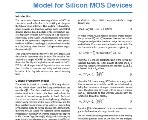 https://silvaco.com/wp-content/uploads/2020/03/simstd_Q2_2014_a1.jpg
1012
782
Ingrid Schwarz
/wp-content/uploads/2019/11/silvaco-logo.png
Ingrid Schwarz2014-04-01 19:23:362021-07-16 21:41:13Generally Applicable Degradation Model for Silicon MOS Devices
https://silvaco.com/wp-content/uploads/2020/03/simstd_Q2_2014_a1.jpg
1012
782
Ingrid Schwarz
/wp-content/uploads/2019/11/silvaco-logo.png
Ingrid Schwarz2014-04-01 19:23:362021-07-16 21:41:13Generally Applicable Degradation Model for Silicon MOS Devices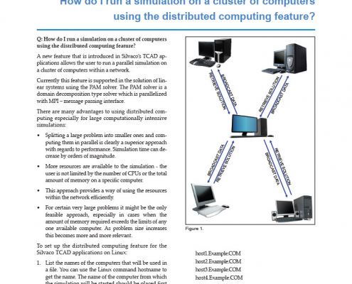 https://silvaco.com/wp-content/uploads/2020/03/simstd_Q1_2014_hints2.jpg
1012
782
Ingrid Schwarz
/wp-content/uploads/2019/11/silvaco-logo.png
Ingrid Schwarz2014-01-01 19:04:132021-07-16 21:41:13Hints, Tips, and Solutions – Simulation on a Cluster of Computers Using the Distributed Computing Feature
https://silvaco.com/wp-content/uploads/2020/03/simstd_Q1_2014_hints2.jpg
1012
782
Ingrid Schwarz
/wp-content/uploads/2019/11/silvaco-logo.png
Ingrid Schwarz2014-01-01 19:04:132021-07-16 21:41:13Hints, Tips, and Solutions – Simulation on a Cluster of Computers Using the Distributed Computing Feature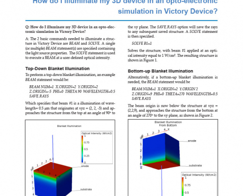 https://silvaco.com/wp-content/uploads/2020/03/simstd_Q1_2014_hints1.jpg
1012
782
Ingrid Schwarz
/wp-content/uploads/2019/11/silvaco-logo.png
Ingrid Schwarz2014-01-01 18:35:432021-07-16 21:41:13Hints, Tips and Solutions – Illuminate a 3D device in a Victory Device Opto-electronic Simulation
https://silvaco.com/wp-content/uploads/2020/03/simstd_Q1_2014_hints1.jpg
1012
782
Ingrid Schwarz
/wp-content/uploads/2019/11/silvaco-logo.png
Ingrid Schwarz2014-01-01 18:35:432021-07-16 21:41:13Hints, Tips and Solutions – Illuminate a 3D device in a Victory Device Opto-electronic Simulation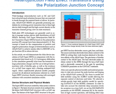 https://silvaco.com/wp-content/uploads/2020/03/simstd_Q1_2014_a2.jpg
1012
782
Ingrid Schwarz
/wp-content/uploads/2019/11/silvaco-logo.png
Ingrid Schwarz2014-01-01 14:52:202021-07-16 21:41:27Atlas Simulation of GaN-Based Super Heterojunction Field Effect Transistors Using the Polarization Junction Concept
https://silvaco.com/wp-content/uploads/2020/03/simstd_Q1_2014_a2.jpg
1012
782
Ingrid Schwarz
/wp-content/uploads/2019/11/silvaco-logo.png
Ingrid Schwarz2014-01-01 14:52:202021-07-16 21:41:27Atlas Simulation of GaN-Based Super Heterojunction Field Effect Transistors Using the Polarization Junction Concept https://silvaco.com/wp-content/uploads/2020/03/simstd_Q1_2014_a1.jpg
1012
782
Ingrid Schwarz
/wp-content/uploads/2019/11/silvaco-logo.png
Ingrid Schwarz2014-01-01 14:46:272021-07-16 21:41:27Modeling the Optical Response of Phonon-dressed Excitons in OLED Simulations
https://silvaco.com/wp-content/uploads/2020/03/simstd_Q1_2014_a1.jpg
1012
782
Ingrid Schwarz
/wp-content/uploads/2019/11/silvaco-logo.png
Ingrid Schwarz2014-01-01 14:46:272021-07-16 21:41:27Modeling the Optical Response of Phonon-dressed Excitons in OLED Simulations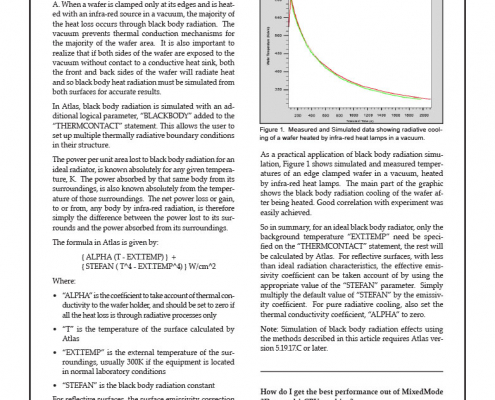 https://silvaco.com/wp-content/uploads/2020/03/simstd_Q4_2013_hints.jpg
1012
782
Ingrid Schwarz
/wp-content/uploads/2019/11/silvaco-logo.png
Ingrid Schwarz2013-10-01 15:29:452021-07-16 21:41:28Hints, Tips, and Solutions – Simulate Rapid Thermal Annealing Temperature Transients in Vacuum
https://silvaco.com/wp-content/uploads/2020/03/simstd_Q4_2013_hints.jpg
1012
782
Ingrid Schwarz
/wp-content/uploads/2019/11/silvaco-logo.png
Ingrid Schwarz2013-10-01 15:29:452021-07-16 21:41:28Hints, Tips, and Solutions – Simulate Rapid Thermal Annealing Temperature Transients in Vacuum