Simulation of a Bipolar Junction Transistor Under High and Low Current Injection Conditions
Semiconductor devices such as bipolar power transistors and solar cells may operate over a range of optical or electrical injection levels. In some cases of high injection, this may result in the occurrence of an electron-hole plasma somewhere in the device. For reliable device simulations, TCAD models need to cover the range of operating conditions and have models which depend on carrier densities, electric field, dopant densities, trap densities, and temperature. For the carrier mobilities, a Silvaco Device Simulator has several models that work well for high doping levels and high free carrier densities. For Shockley-Read-Hall carrier recombination, a Silvaco Device Simulator has a range of options for trying to include the dependence of the recombination lifetimes on dopant densities, and one model to include the dependence on carrier density [1]. At very high carrier concentrations, however, the dominant carrier recombination mechanism is Auger recombination.
Thermo-mechanical Stress in Through-Silicon-Vias
During the last several years, the enhancement of integrated circuits (ICs) performance and power consumption have contributed to the continual scaling down the size of transistors. However, scaling down semiconductor devices has brought serious challenges to the materials and processes of on-chip interconnects beyond the 32-nm technology node. Therefore, some researchers proposed another direction to increase the device density by making ICs into three-dimensional (3D) spaces and the 3D IC stacking has attracted tremendous attention for IC integration in order to reduce wire length and footprint.
Hints, Tips and Solutions – Extract geometric information from 3D process simulation
Q: How do I extract geometric information, such as material thickness or junction depth, from the current 3D process simulation using Victory Process?
TCAD Simulation of Impact Ionization at Cryogenic Temperatures, down to 3 K
Some electronic devices operate at very low, cryogenic temperatures, sometimes as low as 4 K, which is the temperature of liquid helium. Such devices include infra-red (IR) photodetectors or single-photon Avalanche Photo-Diodes (APD) (also known as a Geiger-mode APD or GAPD), based on a reverse biased p-n junction in which a photo-generated carrier can trigger an avalanche current due to the impact ionization mechanism. This device is able to detect low-intensity optical signals, e.g. single photon [1], [2].
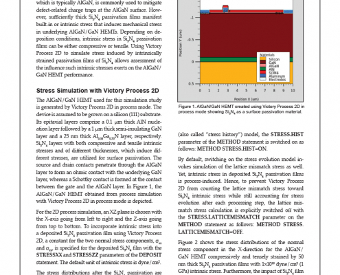
Stress Induced by Intrinsically Strained Silicon Nitride Passivation Films of AlGaN/GaN HEMTs Using Victory Process 2D
In the AlGaN/GaN HEMT fabrication process, silicon nitride (Si3N4) passivation of the HEMT surface layer, which is typically AlGaN, is commonly used to mitigate defect-related charge traps at the AlGaN surface. However, sufficiently thick Si3N4 passivation films manifest built-in or intrinsic stress that induces mechanical stress in underlying AlGaN/GaN HEMTs. Depending on deposition conditions, intrinsic stress in Si3N4 passivation films can be either compressive or tensile. Using Victory Process 2D to simulate stress induced by intrinsically strained passivation films of Si3N4 allows assessment of the influence such intrinsic stresses exerts on the AlGaN/ GaN HEMT performance.
Victory Process 2D – A Valuable Alternative To SUPREM-based Simulators
SUPREM-IV – Stanford University PRocEss Modeling Program was first released 30 years ago. Since then its descendants - Athena from Silvaco and TSUPREM-4TM from TMA/Avant/Synopsys - have been 2D process simulation “work-horses” in semiconductor industry world-wide. Despite the fact that tremendous progress in the industry indeed requires the transition to 3D TCAD there are still many technologies and applications where a 2D simulation is the most practical approach. At the same time, we have to recognize that the SUPREM-based simulators cannot keep up with the progress because they lack many fundamental capabilities required for simulation of modern processes. Victory Process (VP) has been developed by Silvaco to address these challenging requirements. Though ultimate purpose of VP is accurate simulation of complex 3D process it still can be used as a valuable alternative to or even advantageous substitution for SUPREM based simulators. The 2D-mode of Victory Process (VP2D) differs from the full 3D mode only by setting a 2D simulation domain when simulation starts. This means that the same syntax, models, algorithms, layout and the whole process flow can be used in both 2D and 3D. This guarantees smooth transition from 2D to 3D process simulation.
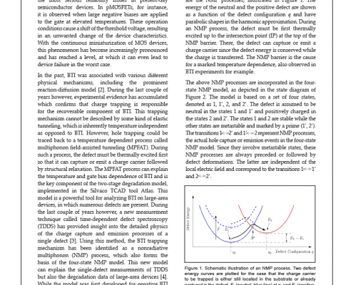
Simulation of Device Degradation Due to Bias Temperature Stress
Introduction Bias Temperature Instability (BTI) [1] ranks among the most serious reliability issues in present-day semiconductor devices. In pMOSFETs, for instance, it is observed when large negative biases are applied to the gate at elevated temperatures. These operation conditions cause a shift of the threshold voltage, resulting in an unwanted change of the device characteristics. With the continuous miniaturization of MOS devices, this phenomenon has become increasingly pronounced and has reached a level, at which it can even lead to device failure in the worst case.
Using Victory Process to Create Realistic Structures for Capacitance Extraction in Clever
Silvaco offers many alternatives for creating simple 3D structures, the optimum choice depending on what the user needs to simulate. Many of the choices for creating simple 3D structures are for user convenience, so that just a single tool can both create the simple 3D structure and simulate the required physics. This gives the user an enhanced feeling of a tightly integrated product.
Hints, Tips and Solutions – How to best visualize vectors and field lines in TonyPlot
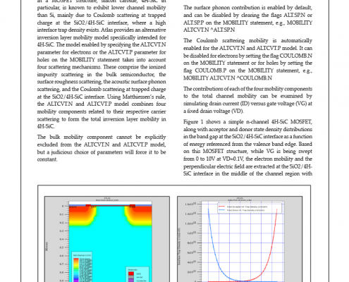
Traditionally, visualizing vectors by means of arrows in TonyPlot was a challenge, especially in the areas where the computational grid was dense. The vector arrows were plotted for every grid point, making them in many cases very hard to discern. One such example is illustrated in Figure 1.
Hints, Tips and Solutions – Scattering mechanisms contributing to reduced channel mobility in 4H-SiC MOSFETs
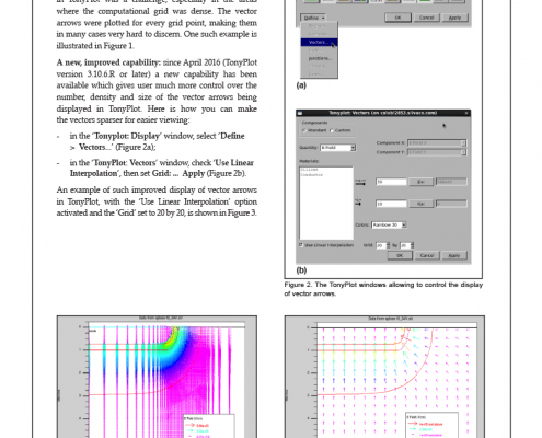
In a MOSFET structure, silicon carbide, 4H-SiC in particular, is known to exhibit lower channel mobility than Si, mainly due to Coulomb scattering at trapped charge at the SiO2/4H-SiC interface, where a high interface trap density exists. Atlas provides an alternative inversion layer mobility model specifically intended for 4H-SiC. The model enabled by specifying the ALTCVT.N parameter for electrons or the ALTCVT.P parameter for holes on the MOBILITY statement takes into account four scattering mechanisms. These comprise the ionized impurity scattering in the bulk semiconductor, the surface roughness scattering, the acoustic surface phonon scattering, and the Coulomb scattering at trapped charge at the SiO2/4H-SiC interface. Using Matthiessen’s rule, the ALTCVT.N and ALTCVT.P model combines four mobility components related to their respective carrier scattering to form the total inversion layer mobility in 4H-SiC.
