Launching Samsung Foundry IP as Silvaco SIPware&What you Need to Know
On Monday, May 13, Silvaco announced that the semiconductor design IP of Samsung Foundry is now marketed, licensed and supported through Silvaco. The addition of Samsung production-proven design IP complements Silvaco’s existing SIPware IP products and solutions—embedded processors, wired interfaces, bus fabrics, peripheral controllers, cores for automotive, consumer and IoT/sensor applications. The initial offering of hard design IP is for the 14nm process node and is expected to extend to advanced technology nodes at 11nm, 10nm and 8nm, as well as mature planar technologies such as 28nm.
Jaehong Park, executive vice president of Design Platform Development Team at Samsung Electronics said this about their design IP: “After identifying the requirements for different consumer, mobile, and HPC applications, we have compiled a full suite of design IPs which include wired and high-speed interfaces, analog and mixed-signal blocks and advanced security hard/soft cores. In partnership with Silvaco, we are bringing our proven IP to SoC engineers world-wide.”
Babak Taheri, CTO and EVP of Products at Silvaco talked about the importance of Samsung IP business: “Silvaco has an established track record, with multiple Tier 1 IP semiconductor companies, to unlock their assets and deliver their captive IP to the market. Silvaco has taken the next step and became a trusted partner of Samsung Foundry. With the launch of their IP we can now offer it to SoC design teams across the world. Design IP is the fastest growing part of Silvaco’s business, and we expect accelerated growth with our Samsung Foundry partnership. I look forward to extending our collaboration with this premier foundry for current and future technology nodes.”
The Samsung Foundry hard and soft design IP will be offered by Silvaco starting in June 2019. If you would like to know more, go to our web-page Samsung Foundry IP.
What’s in the Silvaco SIPware Catalog
Silvaco’s SIPware design IP portfolio is a mix of internal IP from acquisitions, such as SoC Solutions, and partnership with leading System companies. Silvaco has packaged and launched the captive IP from major companies such NXP, TI, Freescale and Infineon to the SoC design marketplace, with Samsung Foundry being the latest. SIPware has been repeatedly proven in production applications.
SIPware is offered in over a dozen different categories spanning both hard (GDS) and soft (RTL) IP types.
For soft IP, the categories include:
- Automotive
- AMBA Cores and Subsystems
- Wired Interfaces
- Security for Safety Applications
SIPware hard IP, with a few exceptions, is from Samsung Foundry. It covers many categories and includes:
- Audio and Video
- Wired and High-Speed Interface
- PLL
- Data Converter
- Regulators and Sensors
- Security for Safety Applications
Samsung Foundry Process Technology
Samsung has consistently held a leading position in the semiconductor industry, and this has now been extended to its foundry business as well. According to IC Insights, Samsung Electronics was the semiconductor market leader in 2018. The reason Samsung has kept its consistent position in the semiconductor industry is its foundry infrastructure. The main backbone of any semiconductor company is ultimately the manufacturing and fab facilities available to it. Its fabrication roadmap includes four FinFET-based processes from 7nm down to 4nm that leverage extreme ultraviolet (EUV) technology as well as 3nm GAA. In the second half of this year, Samsung is scheduled to start the mass production of 6nm process devices and complete the development of 4nm process.
Samsung Foundry’s operations are truly global as well with presence across the world for supporting semiconductor manufacturing, testing, packaging, etc. Samsung is a leader the way in packaging technology development, with many innovations making their debuts in Samsung consumer products. Some of its #1 packaging technologies include:
- World-largest fine pitch flip chip packaging
- World-first through silicon via technology mass production for high-density DRAM
- World-first TSV SiP product development for mobile application processors
- World-best package-on-package technology for smart phones
- World-highest capacity flash memory stacking technologies for SSD
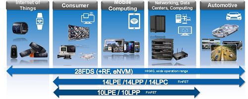
Fig. 1. Applications areas of Samsung Foundry offerings.
A Closer Look at Process Nodes
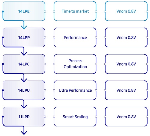
Fig. 2. 14/11nm node process scaling.
14/11nm FinFET
Samsung Foundry introduced the foundry industry’s first 14nm FinFET process technology circa 2013. Samsung Foundry claims several advantages for the process such as the smallest SRAM 14nm bit cell in the industry.
Samsung’s fourth generation 14nm process technology, 14LPU, delivers higher performance at the same power and design rules compared to its Cost-effective third-generation 14nm process (14LPC). 14LPU is suited for high-performance and compute-intensive applications. The 14nm platform covers various applications from high performance (AI, network) to low power(mobile, crypto currency) with.
The Samsung 11LPP process is a hybrid process technology designed to speed up migration from one node to another. Notably, the new node is not a14LPP-based offering featuring 20 nm BEOL (back end of line) interconnects. Instead 11LPP is based on Samsung’s 10 nm BEOL and therefore enables smaller chips than technologies based on Samsung’s 14 nm offerings. Meanwhile, the 11LPP still uses some of the elements featured by Samsung’s 14LPP fabrication process.
Silvaco SIPware has a broad portfolio of 14/11 nm IP.
10/8nm FinFET
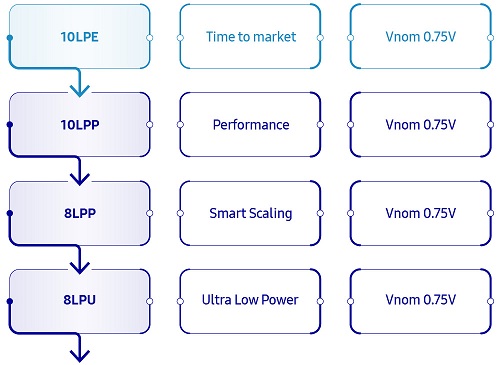
Fig. 3. 10/8nm node process scaling.
Samsung foundry has developed 10nm FinFET technology with an optimized fin structure, stress engineering and cost-effective multi-patterning technology to meet aggressive market requirements. The real benefit of 10nm technology is not just scaling, but also DTCO (Design Technology Co-Optimization) methodology which offer more scalability and better performance than prior nodes. Samsung foundry has evolved the utilization of multi-patterning technology to overcome cost concerns dues to additional masks and it is expected 10nm will have a life-time similar to14nm. The 8LPP node is the most optimized and economical node until EUV availability at 7nm. 8LPU provides ultra-low power with similar switching performance to 7nm.
FD-SOI (Fully Depleted-Silicon on Insulator)
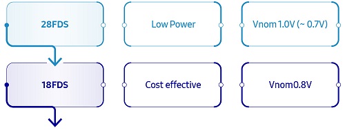
Fig. 4. 28/18nm FD-SOI node process scaling.
Samsung Foundry expects to tape-out more than 20 chips in its 28-nm FD-SOI process this year, as the process now has mature yields and a growing customer set for 28-nm FDS. Application areas for the reported tapeouts include Networking/Computing, Consumer, IoT/Wearable and Automotive/Industrial. The South Korean giant provides design guides for using the body biasing of the process and has automotive Grade 1 capability in place with Grade 2 coming by mid-year. The availability of eMRAM (embedded Magnetic Random Access Memory) technology enables ultra-small bit cell area, superior write speed and endurance time.
18FDS has the same BEOL as the 14nm FinFET process employing double-patterning and is a migration path for MCU and IoT applications.
Packaging Solutions:
Samsung Foundry provides package solutions through a well-built ecosystem with memory suppliers and OSATs (Outsourced Semiconductor Assembly and Test providers) based on 30 years of integration experiences (1 billion parts of PoP are already shipped so far). Samsung Foundry provides chip/package co-design services which enables optimized design from the beginning of the project. Interposer design is also included in the Foundry’s design services for 2.5D application solutions.
Samsung Foundry already provides a leading memory integration package solution in mobile applications. As higher performance and thinner/smaller package solutions are required, next generations of PoP technology are already applied to several mobile devices and under development.
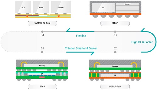
Fig. 5. Samsung Mobile Packaging Solution Flow
High-Speed and Wired-Interface IP
Now that we have an overview of the Samsung Foundry process and packaging solutions, we can look at their specific offerings for high-speed and wired-interface IP. In the table below we see 44 different IPs offered across 5 different process nodes from the SIPware catalog. The performance of the IP meets maximum bandwidth requirements: PCIe up to 16 Gbps, DDR up to 20 Gbps, MIPI M-PHY to 12 Gbps, Ethernet to 56 Gbps, USB / DisplayPort to 5 Gbps and Wi-Fi to 9.2 Gbps.
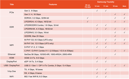
Table 1. SIPware catalog table of Samsung Foundry Interface IP.
Table 1 is just a sample of the available IP. To learn more about Silvaco SIPware for Samsung Foundry, visit Samsung Foundry IP.
