Simulation of Device Degradation Due to Bias Temperature Stress
Introduction Bias Temperature Instability (BTI) [1] ranks among the most serious reliability issues in present-day semiconductor devices. In pMOSFETs, for instance, it is observed when large negative biases are applied to the gate at elevated temperatures. These operation conditions cause a shift of the threshold voltage, resulting in an unwanted change of the device characteristics. With the continuous miniaturization of MOS devices, this phenomenon has become increasingly pronounced and has reached a level, at which it can even lead to device failure in the worst case.
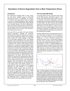
In the past, BTI was associated with various different physical mechanisms, including the prominent reaction-diffusion model [2]. During the last couple of years however, experimental evidence has accumulated which confirms that charge trapping is responsible for the recoverable component of BTI. This trapping mechanism cannot be described by some kind of elastic tunneling, which is inherently temperature independent as opposed to BTI. However, hole trapping could be traced back to a temperature dependent process called multiphonon field-assisted tunneling (MPFAT). During such a process, the defect must be thermally excited first so that it can capture or emit a charge carrier followed by structural relaxation. The MPFAT process can explain the temperature and gate bias dependence of BTI and is the key component of the two-stage degradation model, implemented in the Silvaco TCAD tool Atlas. This model is a powerful tool for analyzing BTI on large-area devices, in which numerous defects are present. During the last couple of years however, a new measurement technique called time-dependent defect spectroscopy (TDDS) has provided insight into the detailed physics of the charge capture and emission processes of a single defect [3]. Using this method, the BTI trapping mechanism has been identified as a nonradiative multiphonon (NMP) process, which also forms the basis of the four-state NMP model. This new model can explain the single-defect measurements of TDDS but also the degradation data of large-area devices [4]. While the model was first developed for negative BTI in pMOSFETs, it has recently been shown to explain all four degradation modes, i.e. negative BTI and positive BTI in n-channel and p-channel MOS transistors [5].


