Optimizing a 2um, 1,500 Volt SiC Superjunction Trench-MOS Device Using TCAD
Abstract
In this paper the critical design features of a SiC superjunction trench MOS device were optimized using CAD to obtain a high breakdown voltage while minimizing any unnecessary increase in channel resistance. The major critical design features of a superjunction trench MOS design were found to be the lateral location of the p-doped pillars with respect to the channel, the thickness and shape of the gate oxide at the bottom of the trench, and the charge balance and doping of the n- and p-doped regions of the superjunction drift region, together with the total depth of this superjunction drift region. The effects of these critical design features on the device characteristics were investigated in turn to arrive at the final near-optimal value of a 1,500 volt breakdown voltage, while still being consistent with a realistic 2um process technology node and vertical channel length. It was clear that other combinations of resistance and breakdown voltage were easily obtainable, but the improvement of one of these figures of merit was always at the expense of the other desirable features.
Introduction
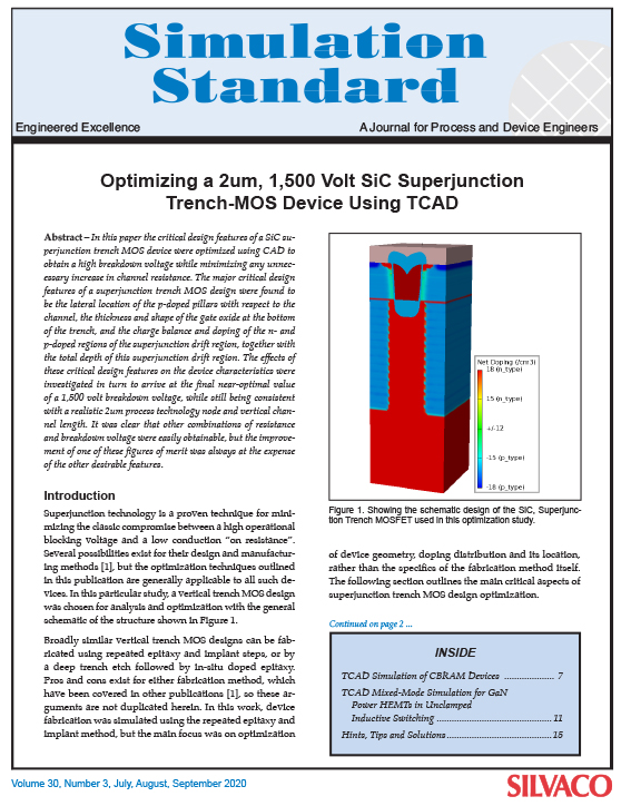
Superjunction technology is a proven technique for minimizing the classic compromise between a high operational blocking voltage and a low conduction “on resistance”. Several possibilities exist for their design and manufacturing methods [1], but the optimization techniques outlined in this publication are generally applicable to all such devices. In this particular study, a vertical trench MOS design was chosen for analysis and optimization with the general
schematic of the structure shown in Figure 1.


