Hints, Tips and Solutions – February 2004
Q. How can I use the EXTRACT commands to find the depletion widths in my MOSFET at different drain biases ?
A. The EXTRACT feature within the DeckBuild application is a powerful feature but requires experience to write the correct syntax. We shall show how it may be used on a structure file to find depletion widths.
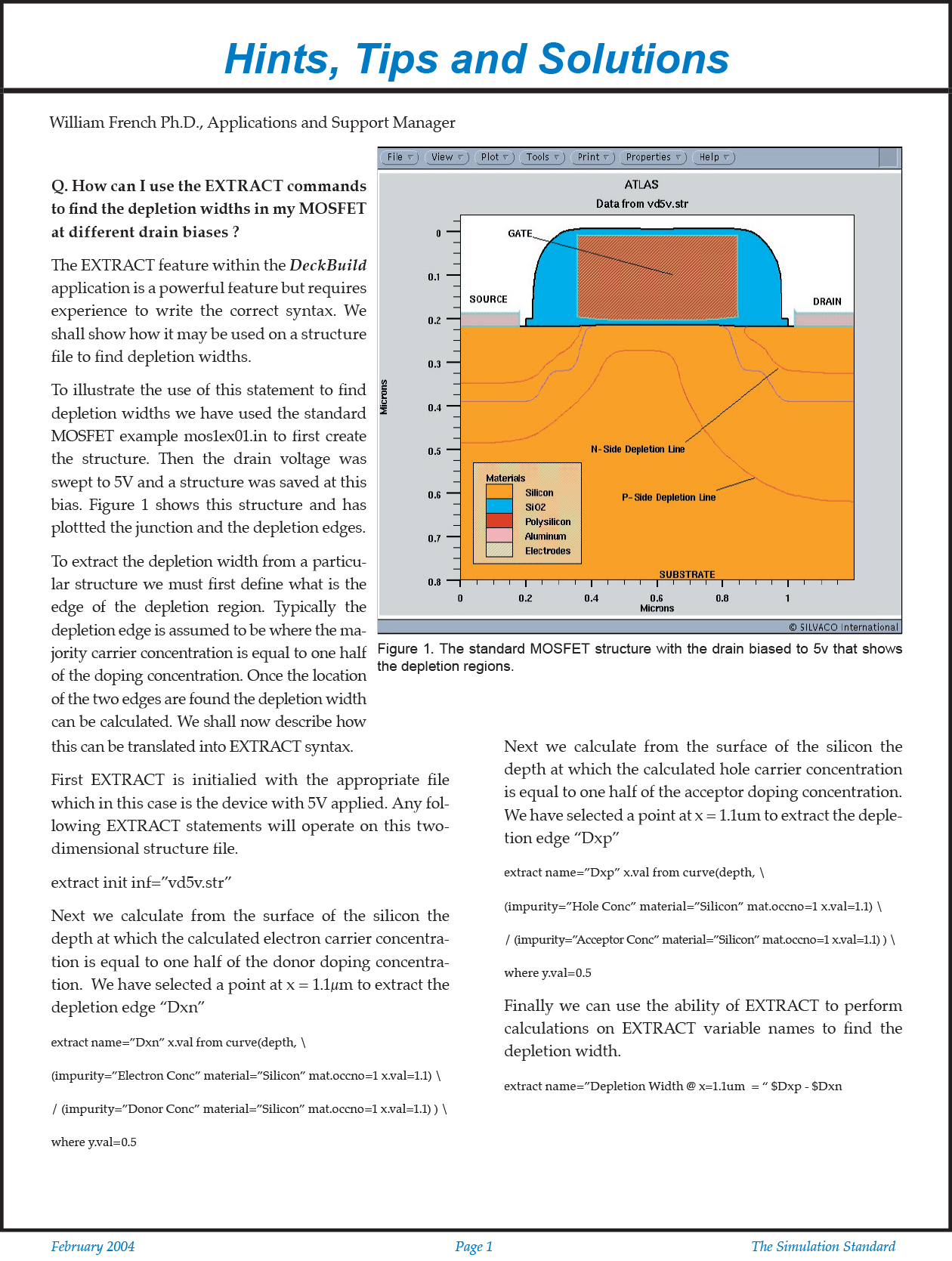
To illustrate the use of this statement to find depletion widths we have used the standard MOSFET example mos1ex01.in to first create the structure. Then the drain voltage was swept to 5V and a structure was saved at this bias. Figure 1 shows this structure and has plottted the junction and the depletion edges.
To extract the depletion width from a particular structure we must first define what is the edge of the depletion region. Typically the depletion edge is assumed to be where the majority carrier concentration is equal to one half of the doping concentration. Once the location of the two edges are found the depletion width can be calculated. We shall now describe how this can be translated into EXTRACT syntax.
First EXTRACT is initialied with the appropriate file which in this case is the device with 5V applied. Any following EXTRACT statements will operate on this two-dimensional structure file.
extract init inf=”vd5v.str”
Next we calculate from the surface of the silicon the depth at which the calculated electron carrier concentration is equal to one half of the donor doping concentration. We have selected a point at x = 1.1µm to extract the depletion edge “Dxn”
extract name=”Dxn” x.val from curve(depth,
(impurity=”Electron Conc” material=”Silicon” mat.occno=1 x.val=1.1)
/ (impurity=”Donor Conc” material=”Silicon” mat.occno=1 x.val=1.1) )where y.val=0.5
Next we calculate from the surface of the silicon the depth at which the calculated hole carrier concentration is equal to one half of the acceptor doping concentration. We have selected a point at x = 1.1um to extract the depletion edge “Dxp”


