Cross-Sectional Viewer
Introduction
With the increase in complexity of IC layouts and processes the designer must have knowledge not only of layout design, but of simulation and manufacturing as well.
Cross-Sectional Viewer is a tool in the Expert layout editor that simulates the cross-sections of ICs along an arbitrary drawn cut-line on the layout. Cross-Sectional Viewer is a link between the layout and the resulting device and it helps the designer to understand its spatial structure. Cross-sectional drawings are useful for detecting parasitic coupling, undesired metal stacking, and other design and fabrication problems.
Expert’s current implementation of Cross-Sectional Viewer is based on a simplified simulation of the process steps using rough processing parameters from the Expert technology file.
Cross-Sectional Viewer Setup
For the simulation of fabrication steps specific parameters must be specified in the technology file. For simplicity we assume that each fabrication step is associated with a separate layer in the layout.
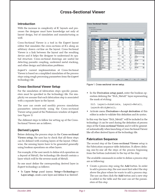
The user can create and modify process simulation parameters interactively using the Cross-sectional Viewer setup panel of the Preferences window of Expert. (see Figure 1)
The different steps to follow for setting up of the Cross-Sectional Viewer are as follows.
Derived Layers
Before defining the process steps in the Cross-sectional Viewer setup, the user has to check that all these steps can be defined with existing layers of the layout. Otherwise, the missing layers have to be generated generally using boolean operations on other layers.
For example, if the user needs to define etch operation on a deposit of Metal1, the technology file should contain a layer which will be the reverse mask of Metal1.
So one must define the corresponding derived layer in Expert technology as follows:
- In Layer Setup panel (menu: Setup>>Technology>> Layer setup), create a new layer and define it as ‘derived’.
- In the Derivation setup panel enter the boolean operation defining the “Etch_Metal1” layer representing the mask of etching:
Dif: Layer1=Substrate, Layer2=Metal1, LayerR=Etch_Metal1;


