Two-Dimensional ATLAS Device Simulation of an Organic Light-Emitting Field-Effect Transistor Using a Heterostructure Inside the Transistor Channel
Sarah Schols, Stijn De Vusser and Paul HeremansIMEC, Kapeldreef 75,B3001 Leuven,Belgium
1. Introduction
Organic semiconductors have been incorporated in a wide range of devices, including organic thin-film transistors (OTFTs) and circuits, organic solar cells, organic non-volatile memories and organic light-emitting diodes (OLEDs). Display applications are a particularly important driver for the further development of this organic technology.
Light-emitting organic field-effect transistors (LEOFETs) may become an interesting structure in this field, as they combine the optical output of an OLED and the gate control of an OTFT in a single device. Therefore, displays based on LEOFETs may eliminate the difficult integration of the light-emitting structure and the organic driving backplane. Moreover, LEOFETs are interesting devices in order to study the opto-electronical properties of organic semiconductors.
Since the first realization of a LEOFET in 2003 [1], LEOFETs have been realized using polymers [2, 3], small molecules [4, 5] and a heterostructure of a p-type and an n-type organic semiconductor [6]. Recently, results were published on LEOFETs based on an ambipolar polymeric semiconductor [7].
Another type of LEOFET comprises a heterojunction inside the transistor channel. In this case excitons are generated at the interface of an n-type and a p-type semiconductor. Therefore, the recombination zone can be located inside the transistor channel, away from the metal source and drain electrodes. More detailed information about the fabrication of this light-emitting transistor can be found elsewhere [8]. In order to understand the basic device operation numerical device simulations are important.
2. The Device Structure
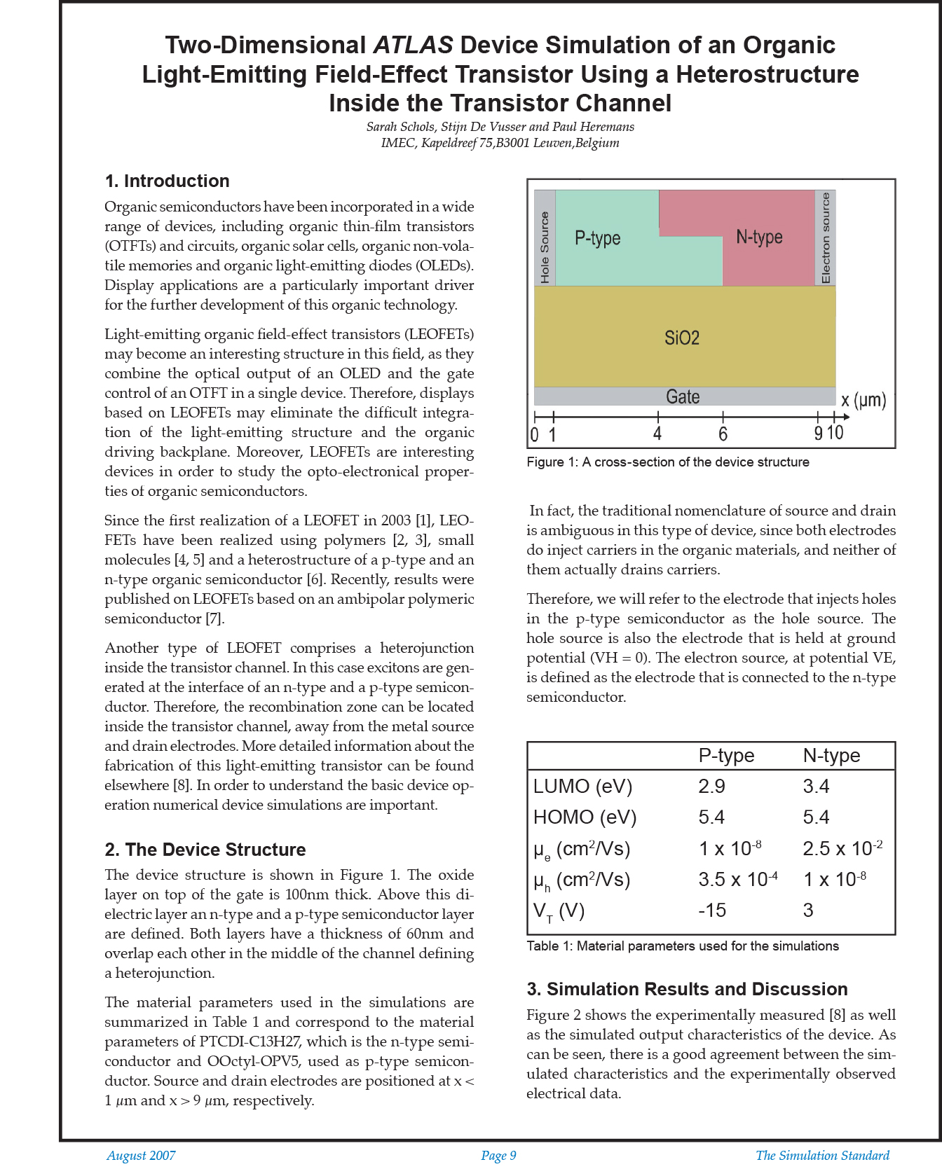
The device structure is shown in Figure 1. The oxide layer on top of the gate is 100nm thick. Above this dielectric layer an n-type and a p-type semiconductor layer are defined. Both layers have a thickness of 60nm and overlap each other in the middle of the channel defining a heterojunction.


