A Semi-Analytical Model for the Subthreshold Behavior of FinFLASH Structures
L. Perniola, J. Razafindramora, P. Scheiblin, F. Daug´e, C. Jahan, B. De Salvo, G. Reimbold, F. Boulanger
CEA-LETI
17, Rue des Martyrs, F&38054, Grenoble, France, luca.perniola@cea.fr
G. Ghibaudo
INP Grenoble MINATEC
3, Parvis Louis N´eel, BP 257, 38016 Grenoble Cedex 1
Abstract
In this paper we present an original semi-analytical model for the subthreshold electrical behavior of complex 3D structures as the SOI FinFLASH devices. This physically-based model, which does not need any fitting parameter, solves the Poisson equation for a fin covered by trapped charges in the active dielectrics. The analytical results are compared with fully 3D numerical simulations and a good agreement is obtained down to fins with very small feature sizes (order of tens of nm). This model can be efficiently used to gain information on important cell electrical behaviors as the threshold voltage shift Vth and the subthreshold slope factor S.
Introduction
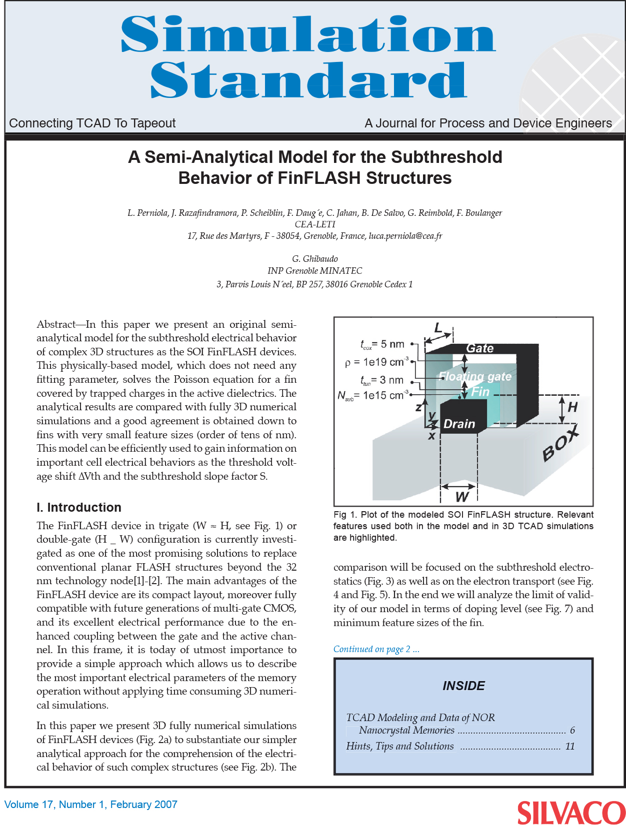
The FinFLASH device in trigate (W ≈ H, see Fig. 1) or double-gate (H _ W) configuration is currently investigated as one of the most promising solutions to replace conventional planar FLASH structures beyond the 32 nm technology node[1]-[2]. The main advantages of the FinFLASH device are its compact layout, moreover fully compatible with future generations of multi-gate CMOS, and its excellent electrical performance due to the enhanced coupling between the gate and the active channel. In this frame, it is today of utmost importance to provide a simple approach which allows us to describe the most important electrical parameters of the memory operation without applying time consuming 3D numerical simulations.


